DCR-PC350/PC350E
4-65
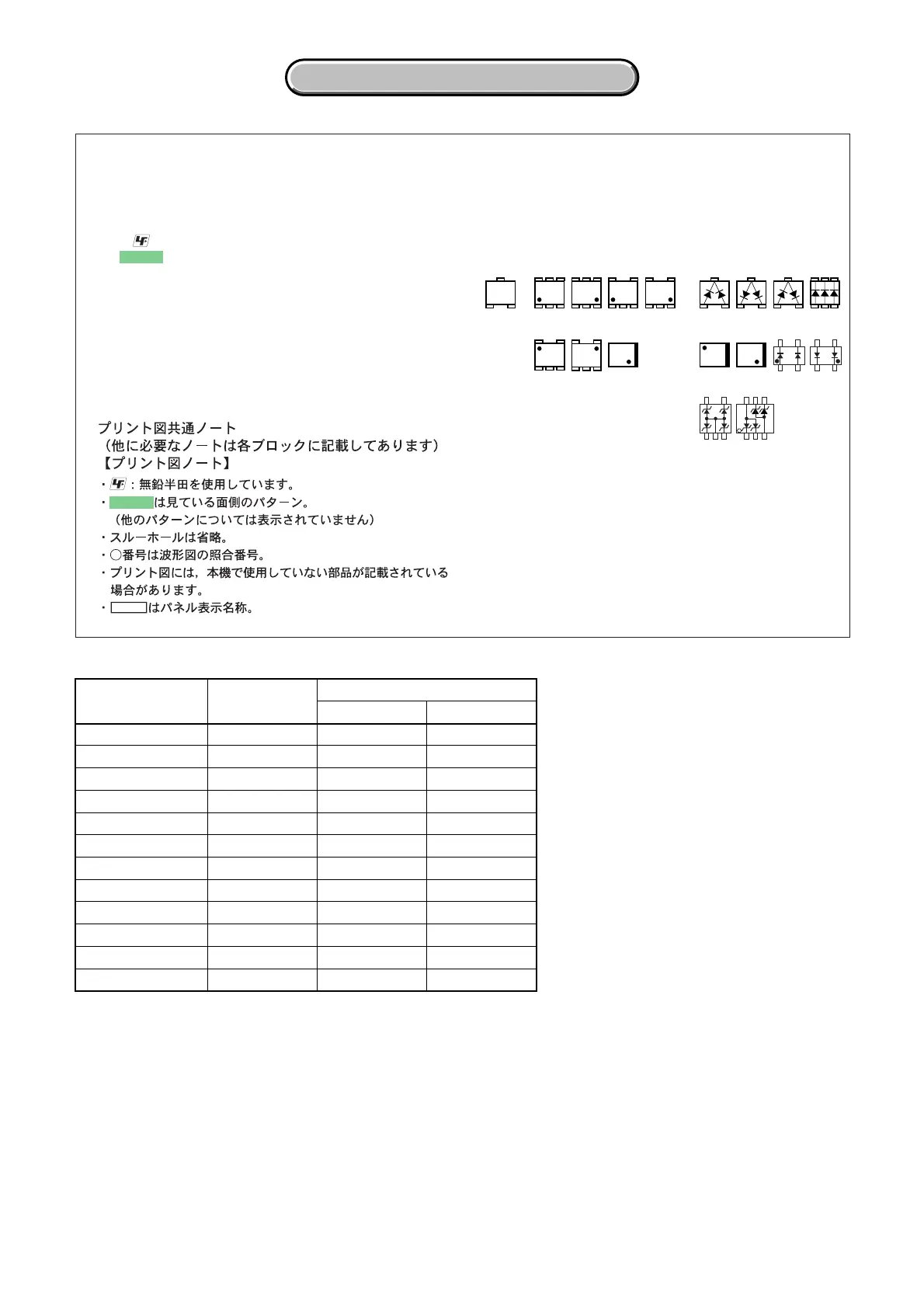
4-3. PRINTED WIRING BOARDS
4-3. PRINTED WIRING BOARDS
(For printed wiring boards)
•
: Uses unleaded solder.
•
: Pattern from the side which enables seeing.
(The other layers’ patterns are not indicated)
• Through hole is omitted.
• Circled numbers refer to waveforms.
• There are a few cases that the part printed on diagram
isn’t mounted in this model.
• C: panel designation
(ENGLISH)
THIS NOTE IS COMMON FOR WIRING BOARDS
(In addition to this, the necessary note is printed in each block)
21
3
21
3
21
3
345
21
123
654
EB
C
31
5
5
2
46
123
54
43
12
5
4
1
3
12
43
312
45
534
12
34
21
12
43
46
2
5
31
12
4
3
64
1
3
• Chip parts
Transistor Diode
(JAPANESE)
board name
CR-048
SE-151
FP-995
VP-060
FP-993
FP-994
MS-234
ST-108
PD-225
FP-996
CD-537
VC-370
parts location
(shown on page)
–
–
–
–
–
–
4-93
4-93
4-93
4-93
4-94
4-94, 95
number of layers
6
6
1
6
1
1
4
4
2
1
6
8
layers not shown
2 to 5
2 to 5
–
2 to 5
–
–
2 to 3
2 to 3
–
–
2 to 5
2 to 7
pattern
BOARD INFORMATION
 Loading...