DocID018909 Rev 11 101/1731
RM0090 Embedded Flash memory interface
112
3.9.5 Flash status register (FLASH_SR) for
STM32F405xx/07xx and STM32F415xx/17xx
The Flash status register gives information on ongoing program and erase operations.
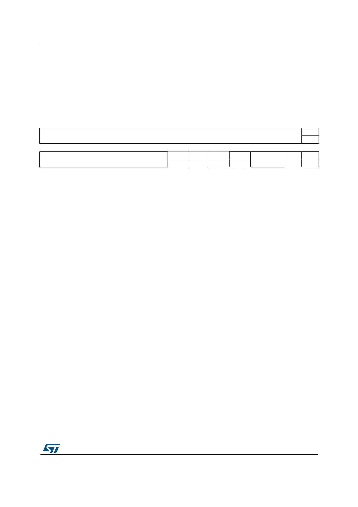
Address offset: 0x0C
Reset value: 0x0000 0000
Access: no wait state, word, half-word and byte access
31 30 29 28 27 26 25 24 23 22 21 20 19 18 17 16
Reserved
BSY
r
15 14 13 12 11 10 9 8 7 6 5 4 3 2 1 0
Reserved
PGSERR PGPERR PGAERR WRPERR
Reserved
OPERR EOP
rc_w1 rc_w1 rc_w1 rc_w1 rc_w1 rc_w1
Bits 31:17 Reserved, must be kept cleared.
Bit 16 BSY: Busy
This bit indicates that a Flash memory operation is in progress. It is set at the beginning of a
Flash memory operation and cleared when the operation finishes or an error occurs.
0: no Flash memory operation ongoing
1: Flash memory operation ongoing
Bits 15:8 Reserved, must be kept cleared.
Bit 7 PGSERR: Programming sequence error
Set by hardware when a write access to the Flash memory is performed by the code while the
control register has not been correctly configured.
Cleared by writing 1.
Bit 6 PGPERR: Programming parallelism error
Set by hardware when the size of the access (byte, half-word, word, double word) during the
program sequence does not correspond to the parallelism configuration PSIZE (x8, x16, x32,
x64).
Cleared by writing 1.
Bit 5 PGAERR: Programming alignment error
Set by hardware when the data to program cannot be contained in the same 128-bit Flash
memory row.
Cleared by writing 1.
Bit 4 WRPERR: Write protection error
Set by hardware when an address to be erased/programmed belongs to a write-protected part
of the Flash memory.
Cleared by writing 1.