DocID018909 Rev 11 553/1731
RM0090 Advanced-control timers (TIM1&TIM8)
581
– CC1P=0 and CC1NP=’0’ in TIMx_CCER register to validate the polarity (and
detect rising edge only).
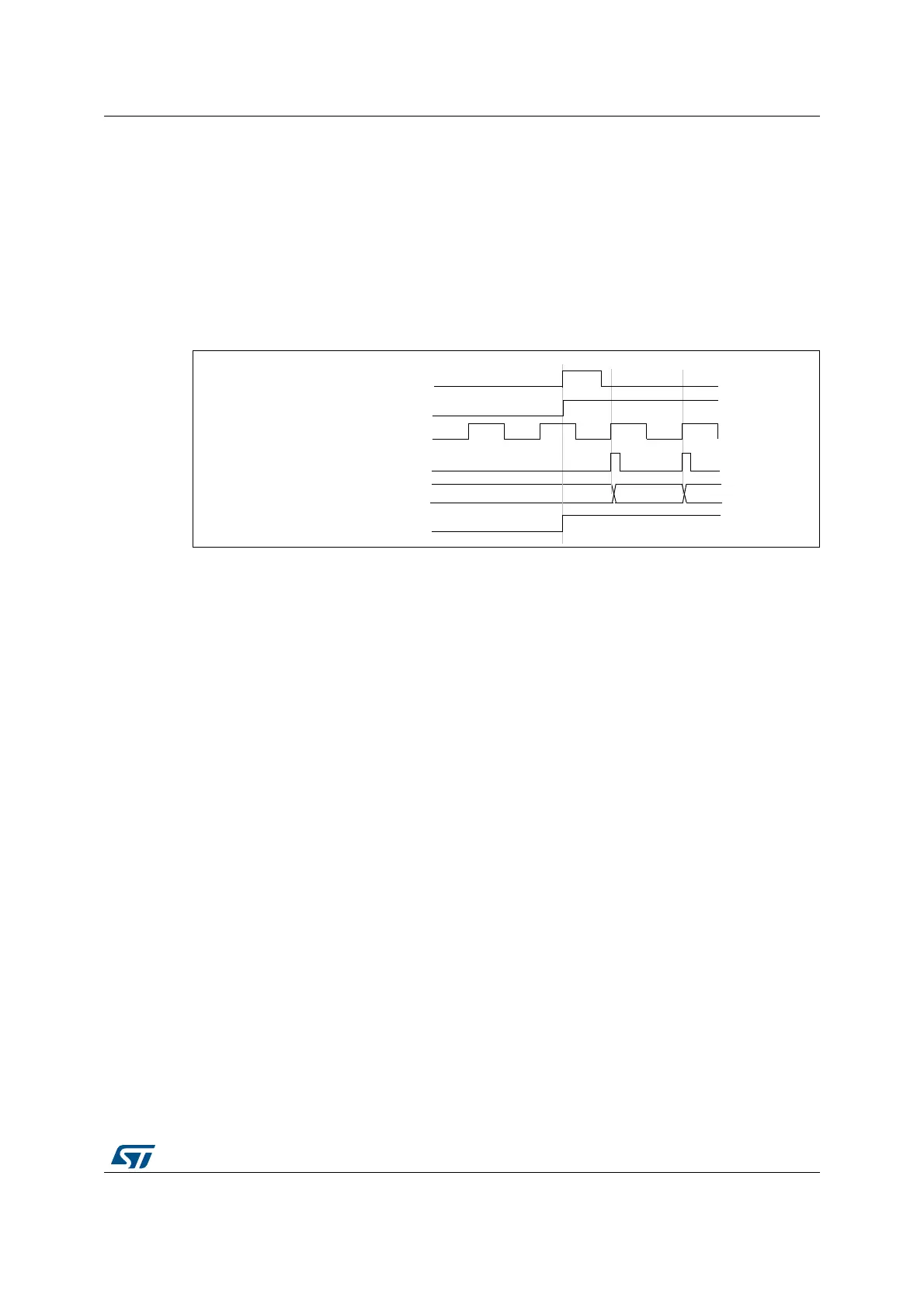
3. Configure the timer in trigger mode by writing SMS=110 in TIMx_SMCR register. Select
TI1 as the input source by writing TS=101 in TIMx_SMCR register.
A rising edge on TI1 enables the counter and sets the TIF flag. The counter then counts on
ETR rising edges.
The delay between the rising edge of the ETR signal and the actual reset of the counter is
due to the resynchronization circuit on ETRP input.
Figure 133. Control circuit in external clock mode 2 + trigger mode
17.3.20 Timer synchronization
The TIM timers are linked together internally for timer synchronization or chaining. Refer to
Section 18.3.15: Timer synchronization on page 612 for details.
Note: The clock of the slave timer must be enabled prior to receive events from the master timer,
and must not be changed on-the-fly while triggers are received from the master timer.
17.3.21 Debug mode
When the microcontroller enters debug mode (Cortex
®
-M4 with FPU core halted), the TIMx
counter either continues to work normally or stops, depending on DBG_TIMx_STOP
configuration bit in DBG module. For more details, refer to Section 38.16.2: Debug support
for timers, watchdog, bxCAN and I2C.
Counter clock = CK_CNT = CK_PSC
Counter register
35 3634
ETR
CEN/CNT_EN
TIF
TI1