DocID018909 Rev 11 1085/1731
RM0090 Controller area network (bxCAN)
1112
A valid edge is defined as the first transition in a bit time from dominant to recessive bus
level provided the controller itself does not send a recessive bit.
If a valid edge is detected in BS1 instead of SYNC_SEG, BS1 is extended by up to SJW so
that the sample point is delayed.
Conversely, if a valid edge is detected in BS2 instead of SYNC_SEG, BS2 is shortened by
up to SJW so that the transmit point is moved earlier.
As a safeguard against programming errors, the configuration of the Bit Timing Register
(CAN_BTR) is only possible while the device is in Standby mode.
Note: For a detailed description of the CAN bit timing and resynchronization mechanism, please
refer to the ISO 11898 standard.
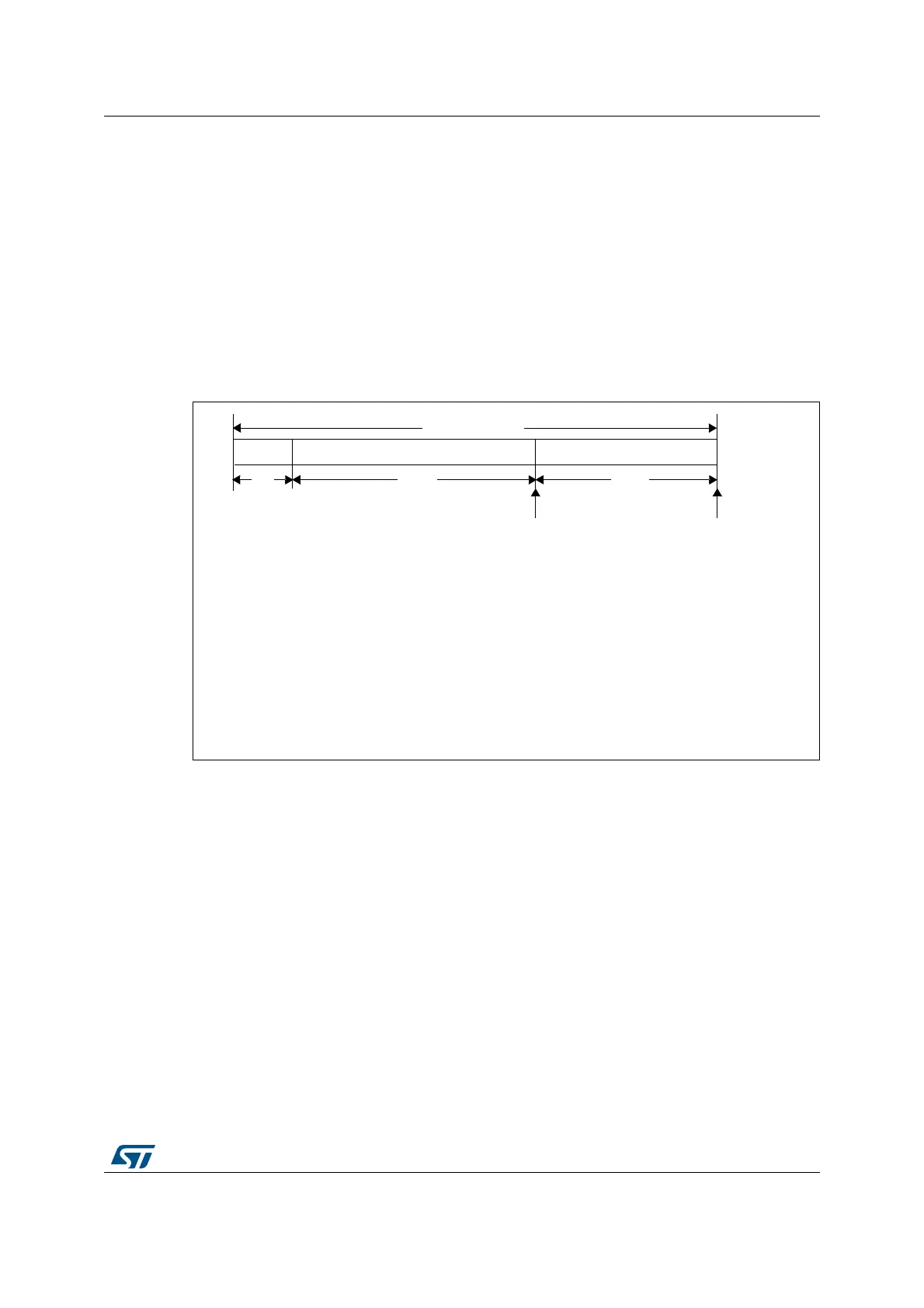
Figure 346. Bit timing
SYNC_SEG BIT SEGMENT 1 (BS1) BIT SEGMENT 2 (BS2)
NOMINAL BIT TIME
1 x t
q
t
BS1
t
BS2
SAMPLE POINT TRANSMIT POINT
NominalBitTime 1 t
q
× t
BS1
t
BS2
++=
with:
t
BS1
= t
q
x (TS1[3:0] + 1),
t
BS2
= t
q
x (TS2[2:0] + 1),
t
q
= (BRP[9:0] + 1) x t
PCLK
t
PCLK
= time period of the APB clock,
BRP[9:0], TS1[3:0] and TS2[2:0] are defined in the CAN_BTR Register.
BaudRate
1
NominalBitTime
----------------------------------------------=
where t
q
refers to the Time quantum
 Loading...