Circuit Descriptions
5–36
1502C MTDR Service Manual
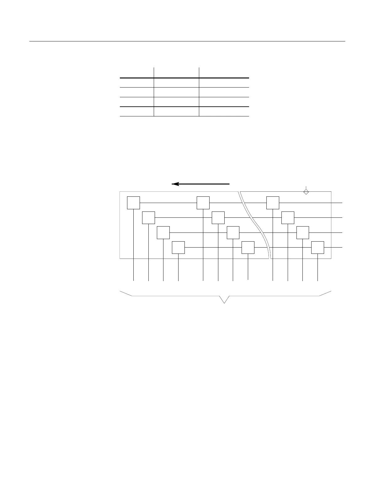
FR Bit X in Latch Column X Output
0 0 V
4
0 1 V
LCD
1 0 V
3
1 1 +5 VDC
The pixels selected by both the column drivers and the row driver are turned on; all
others are off. The process of filling the column drivers is repeated every LP (i.e.,
for every addressed row until all lines in both screen halves have been refreshed).
One frame is thus complete and the entire process is repeated.
Shift Direction
Shift Register Detail
Col X Seg 63
Col X Seg 62 + 1
Xscl
D3
D2
D1
D0
Col X Seg 1 + 63
Col X Seg 0 + 64
Figure 5–20: Shift Register
The display memory is an 8k X 8 RAM (only 4k X 8 is used), located on the Row
Driver/Controller Board. The display memory stores the current bit pattern
generated by the processor on the Main Board. The processor interrupts the
controller periodically and places a new bit pattern in the display memory. The
controller then reads the bit pattern out of the display memory, formats it, and sends
it to the column drivers.
The controller, located on the Row Driver/Controller Board, generates control and
timing signals for the row and column drivers, and formats bit pattern data stored
in the display memory, which is then sent to the column drivers.
Display Memory
Controller
Artisan Technology Group - Quality Instrumentation ... Guaranteed | (888) 88-SOURCE | www.artisantg.com