Circuit Descriptions
1502C MTDR Service Manual
5–15
00 (all 0s) selects 0 dB gain and word FF (all 1s) selects 63.75 dB gain. All
intervening values of 0.25 dB multiples are similarly chosen.
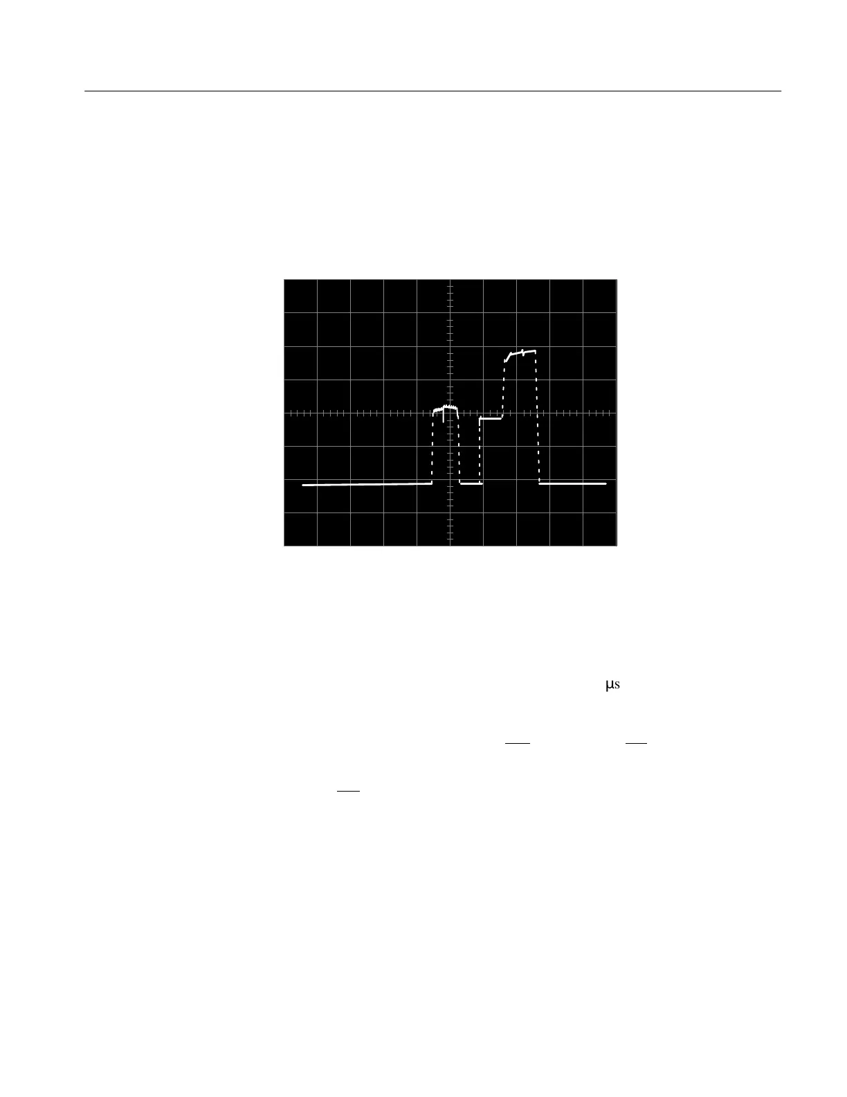
The output of the video amplifier is filtered by R2040 and C2043 for noise
reduction, then sent to the analog-to-digital converter. The output may be observed
at TP4040 (see Figure 5–7).
500mV
20nS
Figure 5–7: Video Processor Output
The output of the video amplifier is converted to its digital equivalent value by ADC
device U2041. The conversion is done using successive approximation technique
to compare the video voltage to the +2.5 VDC reference from U3040. The device
is clocked by a 1.25 MHz clock derived from the timebase oscillator, and completes
its 12-bit plus sign conversion in approximately 100
m
s.
Gate U2040 provides an OR function for the ADC start conversion trigger and read
pulses from the processor system. Either pulse selects the ADC for control and
concurrent pulses select the trigger (WR
input) or read (RD input) functions.
Upon completing a conversion, the processor system is notified by an interrupt
request (IR0
) from U2041.
Timebase
The timebase circuits receive video sample time delay values in digital form from
the processor system and generate precisely timed strobes to the driver/sampler
circuits. Digital counters determine the delay in 50 ns multiples, and analog circuits
further define the delay to fractions of that period. A block diagram of the timebase
circuits is shown in Figure 5–8 (next page).
Video Analog-to-Digital
Converter
Introduction
Artisan Technology Group - Quality Instrumentation ... Guaranteed | (888) 88-SOURCE | www.artisantg.com