Wait
State
Start HIGH
Period
SCL From
Device #1
SCL From
Device #2
Bus Line
SCL
www.ti.com
Operation
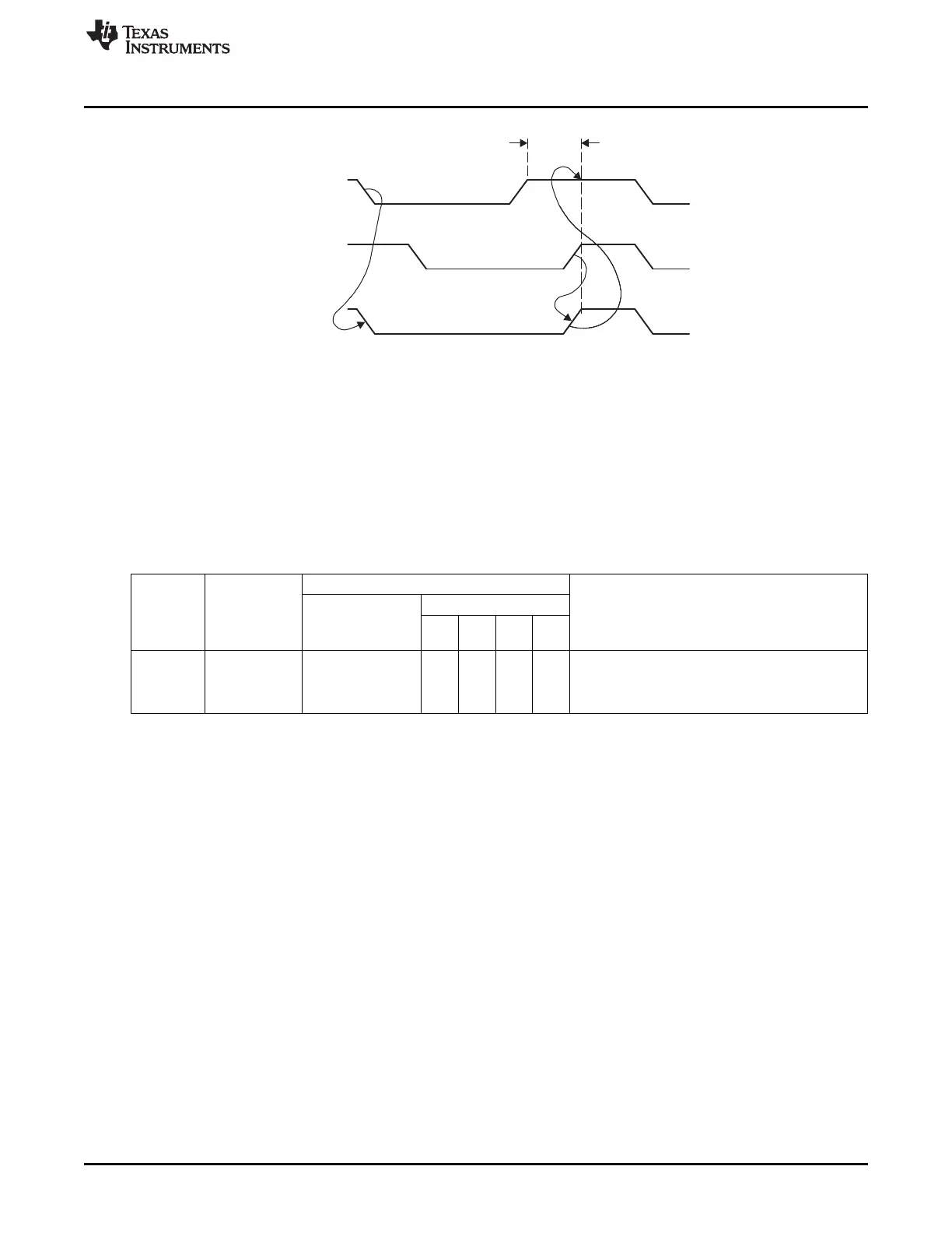
Figure 20-8. Synchronization of Two I
2
C Clock Generators During Arbitration
20.1.6 Bus Error
When an incorrect format of a frame is detected, a bus error condition is entered. The cause is that a
START or STOP condition was detected during transfer of an address, data, or an acknowledge bit. When
a bus error condition is entered, an interrupt is requested. The core leaves the bus error state when the
I2CCFG.STO flag is set and the interrupt request is cleared. It goes into the slave mode and the
I2CCFG.STO flag is automatically reset. The SDA and SCL lines are released (the STOP condition is not
transmitted).
Table 20-5. Miscellaneous States
Status Application Software Response
Code
To I2CCFG
Status of the
(Value of Next Action Taken by I
2
C Hardware
I2C
To/From I2CDATA
I2CSTAT.
STA STO SI AA
STAC)
0x00 Bus error No action 0 1 0 X Only the internal hardware is affected in the MST or
during MST or addressed SLV modes. In all cases, the bus is
selected slave released and I
2
C is switched to the not-addressed
modes SLV mode. The Sto flag is reset.
20.1.7 I
2
C Interrupt
The I
2
C module has an interrupt line to the CPU to signal that it requires service. The I
2
C module uses
interrupt #6, which is also shared with Port 2 inputs; hence, the interrupt routine must also handle Port 2
interrupts if they are enabled.
For an interrupt request to be generated, IEN2.P2IE must be set to 1. When an interrupt request has
been generated, the CPU starts executing the ISR if there are no higher-priority interrupts pending.
An interrupt is generated from the I
2
C module when one of the 26 out of 27 possible I
2
C component states
is entered. The only state that does not cause an interrupt to be generated is state 0xF8, which indicates
that no relevant state information is available. The corresponding I2CCFG.SI flag must be cleared by
software at the end of the ISR.
20.1.8 I
2
C Pins
The SCL and SDA pins of the I
2
C module are connected to pins 2 and 3, respectively, on the
CC2533/CC2541. These pins are pulled up during reset to avoid floating pins. After reset, they are
controlled by the I
2
C module and use an internal pullup resistor of 20 kΩ to hold bus signals high. If these
pins are not to be used for I
2
C, they can be used as GPIO by setting the I2CWC.OVR bit. In this mode,
pins 2 and 3 can be set up as outputs, as inputs with optional pullup, or as 4-mA drive-strength outputs
like the other GPIO pads on the device by using the configuration bits in I2CWC. Their values are read or
controlled using the I2CIO register. These pins cannot be configured to generate GPIO interrupts.
187
SWRU191C–April 2009–Revised January 2012
I
2
C
Submit Documentation Feedback
Copyright © 2009–2012, Texas Instruments Incorporated
 Loading...


