www.ti.com
Debug Commands
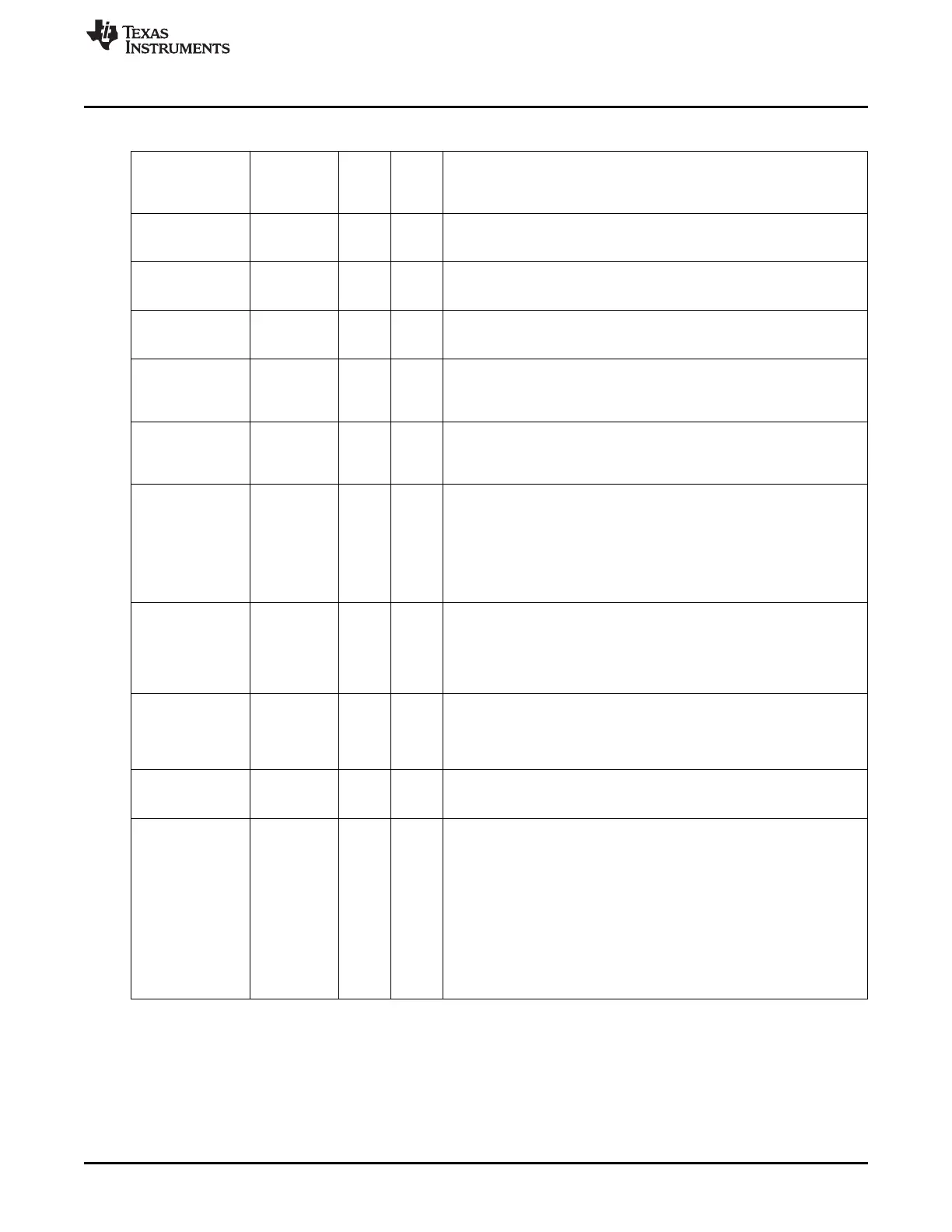
Table 3-1. Debug Commands (continued)
Additi Output
Instruction onal Bytes
Command Description
Byte Input
Bytes
GET_PC 00101XXX 0 2 Return value of 16-bit program counter.
Input byte: none
Output bytes: Returns 2 bytes.
READ_STATUS 00110XXX 0 1 Read status byte.
Input byte: none
Output byte: Debug status byte. See Table 3-3.
SET_HW_BRKPNT 00111XXX 3 1 Set hardware breakpoint.
Input bytes: See Section 3.3.3 for details.
Output byte: Debug status byte. See Table 3-3.
HALT 01000XXX 0 1 Halt CPU operation
Input byte: none
Output byte: Debug status byte. See Table 3-3. If the CPU was already
halted, the output is undefined.
RESUME 01001XXX 0 1 Resume CPU operation. The CPU must be in the halted state for this
command to be run.
Input byte: none
Output byte: Debug status byte. See Table 3-3.
DEBUG_INSTR 01010Xyy 1–3 1 Run debug instruction. The supplied instruction is executed by the CPU
without incrementing the program counter. The CPU must be in halted
state for this command to be run. Note that yy is number of bytes following
the command byte, i.e., how many bytes the CPU instruction has (see
Table 2-3).
Input byte(s): CPU instruction
Output byte: The resulting accumulator register value after the instruction
has been executed
STEP_INSTR 01011XXX 0 1 Step CPU instruction. The CPU executes the next instruction from
program memory and increments the program counter after execution. The
CPU must be in the halted state for this command to be run.
Input byte: none
Output byte: The resulting accumulator register value after the instruction
has been executed
GET_BM 01100XXX 0 1 This command does the same thing as GET_PC, except that it returns the
memory bank. It returns one byte, where the 3 least-significant bits are the
currently used memory bank.
Input byte: none
Output byte: Memory bank (current value of FMAP.MAP)
GET_CHIP_ID 01101XXX 0 2 Return value of 16-bit chip ID and version number.
Input byte: none.
Output bytes: The CHIPID and CHVER register values
BURST_WRITE 10000kkk 2–2049 1
This command writes a sequence of 1–2048 bytes to the DBGDATA
register. Each time the register is updated, a DBG_BW DMA trigger is
generated.
The number of parameters to the BURST_WRITE command is variable.
The number of data bytes in the burst is indicated using the 3 last bits of
the command byte (kkk), and the whole next byte. The command
sequence is shown in Figure 3-5. The burst length is indicated by an 11-bit
value (b10–b0). After these two bytes, the given number of data bytes
must be appended. The value 0 means 2048 data bytes; thus, the smallest
number of bytes to transfer is 1.
Input bytes: Command sequence
Output byte: Debug status byte. See Table 3-3.
57
SWRU191C–April 2009–Revised January 2012 Debug Interface
Submit Documentation Feedback
Copyright © 2009–2012, Texas Instruments Incorporated
 Loading...


