Time
8 Cycles
Debug
Clock
Debug
Data
DataPad
Direction
Cmd Byte
Data Byte 1 Data Byte 2
Output Byte
Input Input
Output
T0305-01
Startof
Command
Sequence
PadIsOutput,But
Chip IsNotReadyto
Respond
Startto
Change
Direction
End of
Command
Sequence
The LevelIs Sampled.
Result=Ready
ChipIsReadyto
ProvideResponse
The LevelIsSampled.
Result=NotReady
t
sample_wait
t
dir_change
Debug Commands
www.ti.com
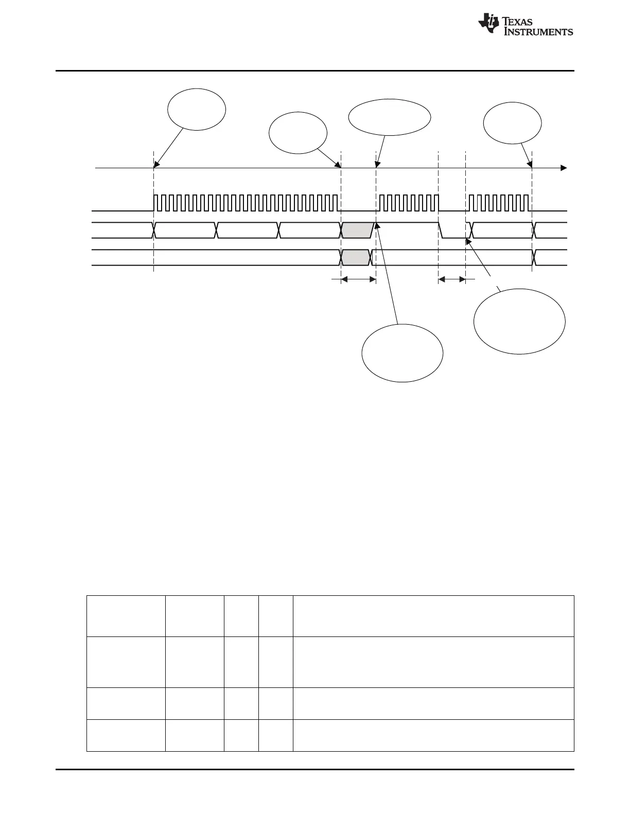
Figure 3-4. Typical Command Sequence. Wait for Response
If the debug interface indicates by pulling the data line high that it is not ready to return data, the external
device must issue exactly eight clock pulses before it samples the ready level again. This must be
repeated until the level is low. The wait cycle is equivalent to reading a byte from the debug interface, but
ignoring the result. Note that the pad starts to change direction on the falling edge of the debug clock.
Thus, the pad driver drives against the driver in the programmer until the programmer changes pad
direction. This duration should be minimized in a programmer implementation.
3.3 Debug Commands
The debug commands are shown in Table 3-1. Some of the debug commands are described in further
detail in the following subsections.
The 3 least-significant bits (the Xs) are don't care values.
Table 3-1. Debug Commands
Additi Output
Instruction onal Bytes
Command Description
Byte Input
Bytes
CHIP_ERASE 00010XXX 0 1 Perform flash chip erase (mass erase) and clear lock bits. If any other
command except READ_STATUS is issued, then the use of CHIP_ERASE
is disabled.
Input byte: none
Output byte: Debug status byte. See Table 3-3.
WR_CONFIG 00011XXX 1 1 Write debug configuration data.
Input byte: See Table 3-2 for details.
Output byte: Debug status byte. See Table 3-3.
RD_CONFIG 00100XXX 0 1 Read debug configuration data.
Input byte: none.
Output byte: Returns value set by WR_CONFIG command. See Table 3-2.
56
Debug Interface SWRU191C–April 2009–Revised January 2012
Submit Documentation Feedback
Copyright © 2009–2012, Texas Instruments Incorporated
 Loading...


