www.ti.com
USB Registers
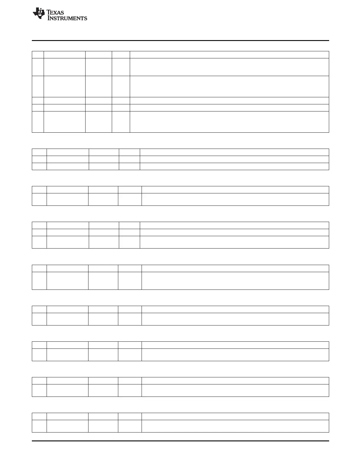
USBCSOH (0x6215) – OUT EP{1–5} Control and Status, High
Bit Name Reset R/W Description
7
AUTOCLEAR
0 R/W When this bit is set to 1, the USBCSOL.OUTPKT_RDY bit is automatically cleared when a
data packet of maximum size (specified by USBMAXO) has been unloaded to the OUT
FIFO.
6
ISO
0 R/W Selects OUT endpoint type
0 Bulk/interrupt
1 Isochronous
5:4 00 R/W Reserved. Always write 00
3:1 – R0 Reserved
0
OUT_DBL_BUF
0 R/W Double buffering enable (OUT FIFO)
0 Double buffering disabled
1 Double buffering enabled
USBCNT0 (0x6216) – Number of Received Bytes in EP0 FIFO (USBINDEX = 0)
Bit Name Reset R/W Description
7:6 – – R0 Reserved
5:0
USBCNT0[5:0]
00 0000 R Number of received bytes into EP 0 FIFO. Only valid when OUTPKT_RDY is asserted
USBCNTL (0x6216) – Number of Bytes in EP{1–5} OUT FIFO, Low
Bit Name Reset R/W Description
7:0
USBCNT[7:0]
0x00 R
8 lsbs of number of received bytes in OUT FIFO selected by USBINDEX register. Only
valid when USBCSOL.OUTPKT_RDY is asserted.
USBCNTH (0x6217) – Number of Bytes in EP{1–5} OUT FIFO, High
Bit Name Reset R/W Description
7:3 – – R0 Reserved
2:0
USBCNT[10:8]
000 R
3 msbs of number of received bytes in OUT FIFO selected by USBINDEX register. Only
valid when USBCSOL.OUTPKT_RDY is set
USBF0 (0x6220) – Endpoint-0 FIFO
Bit Name Reset R/W Description
7:0
USBF0[7:0]
0x00 R/W Endpoint 0 FIFO. Reading this register unloads one byte from the EP0 FIFO. Writing to
this register loads one byte into the EP0 FIFO.
Note: The FIFO memory for EP0 is used for both incoming and outgoing data packets.
USBF1 (0x6222) – Endpoint-1 FIFO
Bit Name Reset R/W Description
7:0
USBF1[7:0]
0x00 R/W Endpoint 1 FIFO register. Reading this register unloads one byte from the EP1 OUT
FIFO. Writing to this register loads one byte into the EP1 IN FIFO.
USBF2 (0x6224) – Endpoint-2 FIFO
Bit Name Reset R/W Description
7:0
USBF2[7:0]
0x00 R/W Endpoint 2 FIFO register. Reading this register unloads one byte from the EP2 OUT
FIFO. Writing to this register loads one byte into the EP2 IN FIFO.
USBF3 (0x6226) – Endpoint-3 FIFO
Bit Name Reset R/W Description
7:0
USBF3[7:0]
0x00 R/W Endpoint 3 FIFO register. Reading this register unloads one byte from the EP3 OUT
FIFO. Writing to this register loads one byte into the EP3 IN FIFO.
USBF4 (0x6228) – Endpoint-4 FIFO
Bit Name Reset R/W Description
7:0
USBF4[7:0]
0x00 R/W Endpoint 4 FIFO register. Reading this register unloads one byte from the EP4 OUT
FIFO. Writing to this register loads one byte into the EP4 IN FIFO.
205
SWRU191C–April 2009–Revised January 2012 USB Controller
Submit Documentation Feedback
Copyright © 2009–2012, Texas Instruments Incorporated

 Loading...