88
MSP430G2452 has one Timer A3 module and so it has three CC channels. Likewise, MSP430G2553 has
six CC channels. When it comes to extreme engineering, TI sometimes seems to overengineer their
products. For example, CC channels are not hard fixed to dedicated pins only unlike other micros. Each
CC channel has a set of pins associated with it and so they can be remapped if needed. Shown below
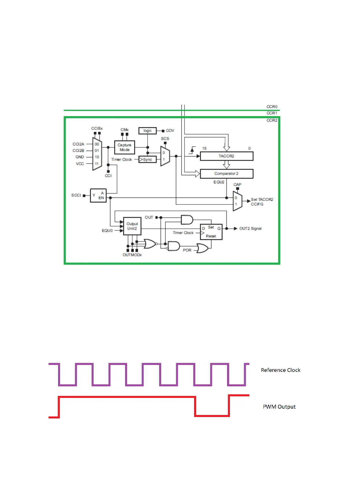
is the block diagram of a Timer A3 CC channel. The left side of the diagram has all the components for
input capture while the right side is intended for compare-match or PWM output. Common to both is
the TACCRn block. It is a very important block.
The basic theme of PWM generation as with any microcontroller is to change the logic state of an
output pin when the count in it associated TACCR register matches with the count in its timer’s counter
register – simply like a binary comparator. This process is called compare-match process. This is
exactly the same idea used in MSP430s. Check the rudimentary timing diagram below. For five
successive falling edges of the reference clock, the PWM output is high and for one edge, the output
is low, resulting in about 83% duty cycle. The reference clock here is actually the timer clock and the
comparison is done by comparing the count stored in TACCRn. Varying TACCRn’s count results in duty
cycle change.