TMS320F2810, TMS320F2811, TMS320F2812
TMS320C2810, TMS320C2811, TMS320C2812
SPRS174T –APRIL 2001–REVISED MAY 2012
www.ti.com
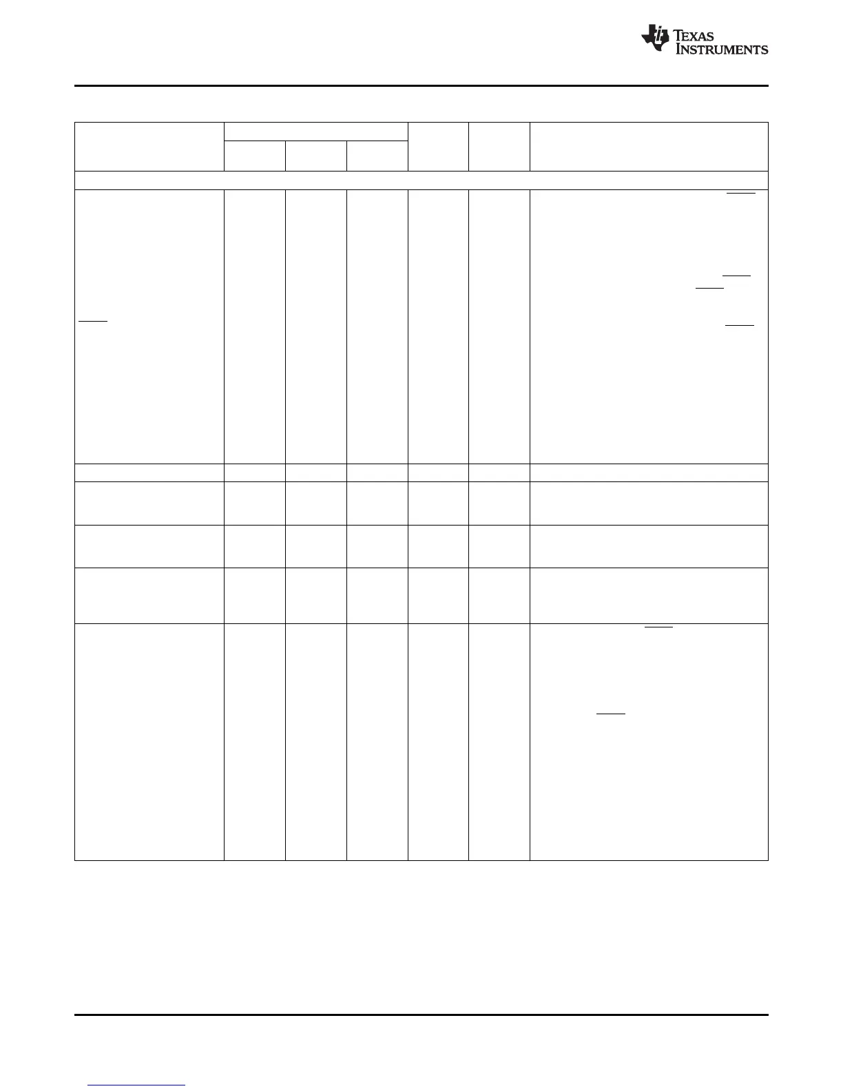
Table 2-2. Signal Descriptions
(1)
(continued)
PIN NO.
NAME I/O/Z
(2)
PU/PD
(3)
DESCRIPTION
179-BALL 176-PIN 128-PIN
GHH/ZHH PGF PBK
JTAG
JTAG test reset with internal pulldown. TRST,
when driven high, gives the scan system
control of the operations of the device. If this
signal is not connected or driven low, the
device operates in its functional mode, and the
test reset signals are ignored.
NOTE: Do not use pullup resistors on TRST; it
has an internal pulldown device. TRST is an
active-high test pin and must be maintained
low at all times during normal device
TRST B12 135 98 I PD
operation. In a low-noise environment, TRST
may be left floating. In other instances, an
external pulldown resistor is highly
recommended. The value of this resistor
should be based on drive strength of the
debugger pods applicable to the design. A 2.2-
kΩ resistor generally offers adequate
protection. Since this is application-specific, it
is recommended that each target board be
validated for proper operation of the debugger
and the application.
TCK A12 136 99 I PU JTAG test clock with internal pullup
JTAG test-mode select (TMS) with internal
TMS D13 126 92 I PU pullup. This serial control input is clocked into
the TAP controller on the rising edge of TCK.
JTAG test data input (TDI) with internal pullup.
TDI C13 131 96 I PU TDI is clocked into the selected register
(instruction or data) on a rising edge of TCK.
JTAG scan out, test data output (TDO). The
contents of the selected register (instruction or
TDO D12 127 93 O/Z –
data) is shifted out of TDO on the falling edge
of TCK.
Emulator pin 0. When TRST is driven high,
this pin is used as an interrupt to or from the
emulator system and is defined as input/output
through the JTAG scan. This pin is also used
to put the device into boundary-scan mode.
With the EMU0 pin at a logic-high state and
the EMU1 pin at a logic-low state, a rising
edge on the TRST pin would latch the device
into boundary-scan mode.
EMU0 D11 137 100 I/O/Z PU
NOTE: An external pullup resistor is
recommended on this pin. The value of this
resistor should be based on the drive strength
of the debugger pods applicable to the design.
A 2.2-kΩ to 4.7-kΩ resistor is generally
adequate. Since this is application-specific, it
is recommended that each target board be
validated for proper operation of the debugger
and the application.
20 Introduction Copyright © 2001–2012, Texas Instruments Incorporated
Submit Documentation Feedback
Product Folder Link(s): TMS320F2810 TMS320F2811 TMS320F2812 TMS320C2810 TMS320C2811 TMS320C2812