TMS320F2810, TMS320F2811, TMS320F2812
TMS320C2810, TMS320C2811, TMS320C2812
www.ti.com
SPRS174T –APRIL 2001–REVISED MAY 2012
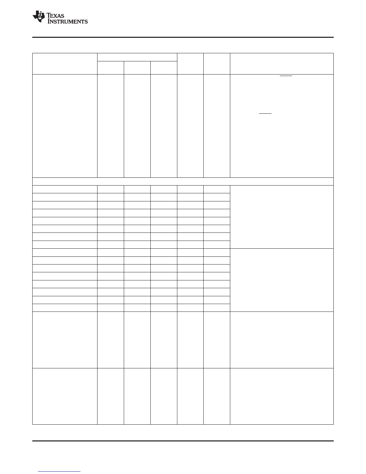
Table 2-2. Signal Descriptions
(1)
(continued)
PIN NO.
NAME I/O/Z
(2)
PU/PD
(3)
DESCRIPTION
179-BALL 176-PIN 128-PIN
GHH/ZHH PGF PBK
Emulator pin 1. When TRST is driven high,
this pin is used as an interrupt to or from the
emulator system and is defined as input/output
through the JTAG scan. This pin is also used
to put the device into boundary-scan mode.
With the EMU0 pin at a logic-high state and
the EMU1 pin at a logic-low state, a rising
edge on the TRST pin would latch the device
into boundary-scan mode.
EMU1 C9 146 105 I/O/Z PU
NOTE: An external pullup resistor is
recommended on this pin. The value of this
resistor should be based on the drive strength
of the debugger pods applicable to the design.
A 2.2-kΩ to 4.7-kΩ resistor is generally
adequate. Since this is application-specific, it
is recommended that each target board be
validated for proper operation of the debugger
and the application.
ADC ANALOG INPUT SIGNALS
ADCINA7 B5 167 119 I –
ADCINA6 D5 168 120 I –
ADCINA5 E5 169 121 I –
8-channel analog inputs for
ADCINA4 A4 170 122 I –
Sample-and-Hold A. The ADC pins should not
be driven before the V
DDA1
, V
DDA2
, and V
DDAIO
ADCINA3 B4 171 123 I –
pins have been fully powered up.
ADCINA2 C4 172 124 I –
ADCINA1 D4 173 125 I –
ADCINA0 A3 174 126 I –
ADCINB7 F5 9 9 I –
ADCINB6 D1 8 8 I –
ADCINB5 D2 7 7 I –
8-channel analog inputs for
ADCINB4 D3 6 6 I –
Sample-and-Hold B. The ADC pins should not
be driven before the V
DDA1
, V
DDA2
, and V
DDAIO
ADCINB3 C1 5 5 I –
pins have been fully powered up.
ADCINB2 B1 4 4 I –
ADCINB1 C3 3 3 I –
ADCINB0 C2 2 2 I –
ADC Voltage Reference Output (2 V).
Requires a low ESR (under 1.5 Ω) ceramic
bypass capacitor of 10 µF to analog ground.
[Can accept external reference input (2 V) if
the software bit is enabled for this mode.
ADCREFP E2 11 11 I/O –
1–10 µF low ESR capacitor can be used in the
external reference mode.]
NOTE: Use the ADC Clock rate to derive the
ESR specification from the capacitor data
sheet that is used in the system.
ADC Voltage Reference Output (1 V).
Requires a low ESR (under 1.5 Ω) ceramic
bypass capacitor of 10 µF to analog ground.
[Can accept external reference input (1 V) if
the software bit is enabled for this mode.
ADCREFM E4 10 10 I/O –
1–10 µF low ESR capacitor can be used in the
external reference mode.]
NOTE: Use the ADC Clock rate to derive the
ESR specification from the capacitor data
sheet that is used in the system.
Copyright © 2001–2012, Texas Instruments Incorporated Introduction 21
Submit Documentation Feedback
Product Folder Link(s): TMS320F2810 TMS320F2811 TMS320F2812 TMS320C2810 TMS320C2811 TMS320C2812
 Loading...