EasyManuals Logo

Xilinx Spartan-6 FPGA Series User Manual

Xilinx Spartan-6 FPGA Series
72 pages
To Next Page IconTo Next Page
To Previous Page IconTo Previous Page
Page #34 background imageLoading...
Page #34 background image
34 www.xilinx.com Spartan-6 FPGA PCB Design and Pin Planning
UG393 (v1.1) April 29, 2010
Chapter 2: Power Distribution System
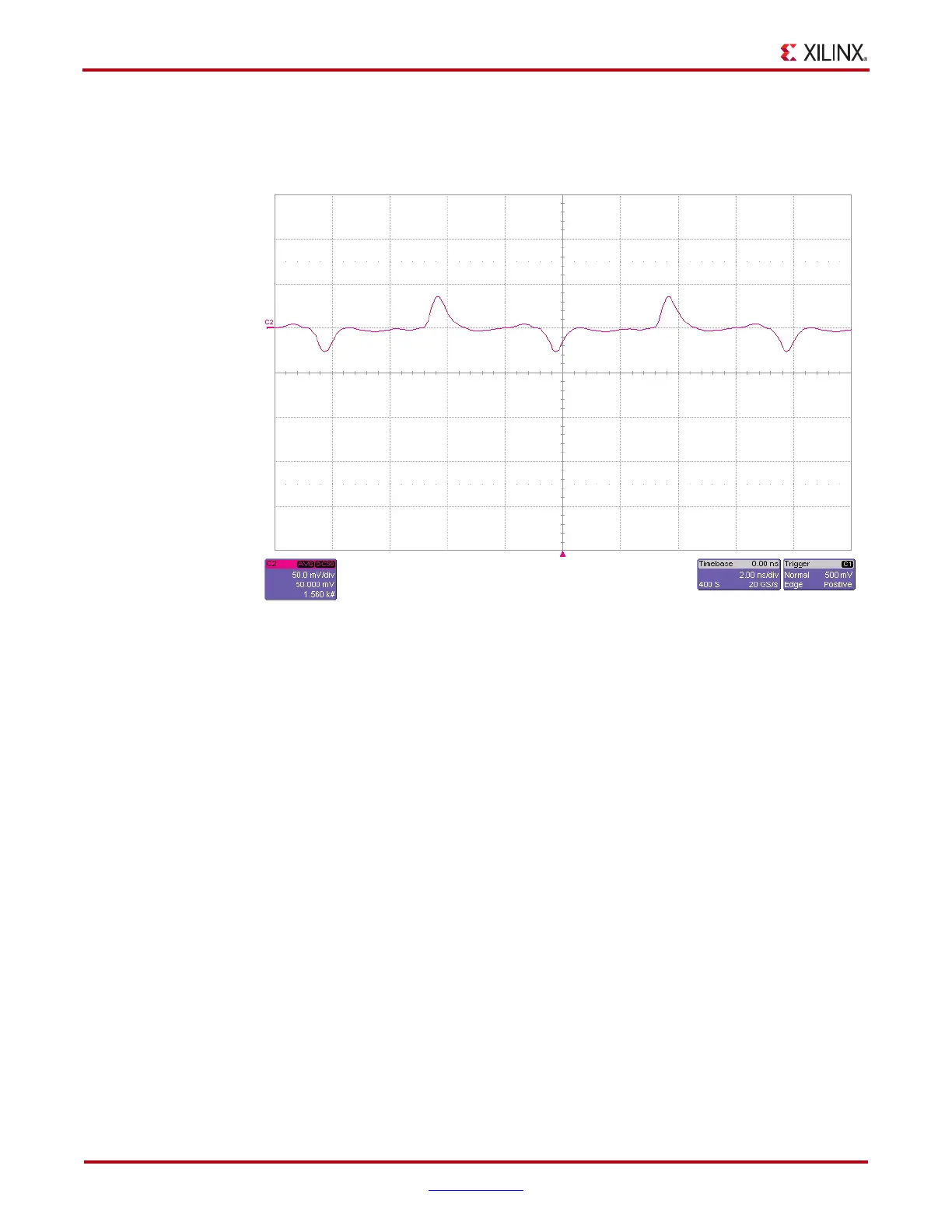
Figure 2-9 shows an averaged noise measurement taken at the V
CCO
pins of a sample
design. In this case, the trigger was the clock for an I/O bus interface sending a 1-0-1-0
pattern at 250 Mb/s.
X-Ref Target - Figure 2-9
Figure 2-9: Averaged Measurement of V
CCO
Supply with Multiple I/O Sending
Patterns at 250 Mb/s
ug393_c2_09_091809

Table of Contents

Questions and Answers:

Question and Answer IconNeed help?

Do you have a question about the Xilinx Spartan-6 FPGA Series and is the answer not in the manual?

Xilinx Spartan-6 FPGA Series Specifications

General IconGeneral
Device FamilySpartan-6
CategoryFPGA
Number of Logic Cells3, 840 to 147, 443
Block RAM216 Kb to 4, 824 Kb
Maximum User I/O102 to 576
Process Technology45nm
Operating Voltage1.2V
Number of DSP Slices8 to 180
Package OptionsFG256, FG484, FG676, FG900, FG1156, FT256, FTG256, FTG484, FTG676, FTG900, FTG1156

Related product manuals