MC96F6432
100 June 22, 2018 Ver. 2.9
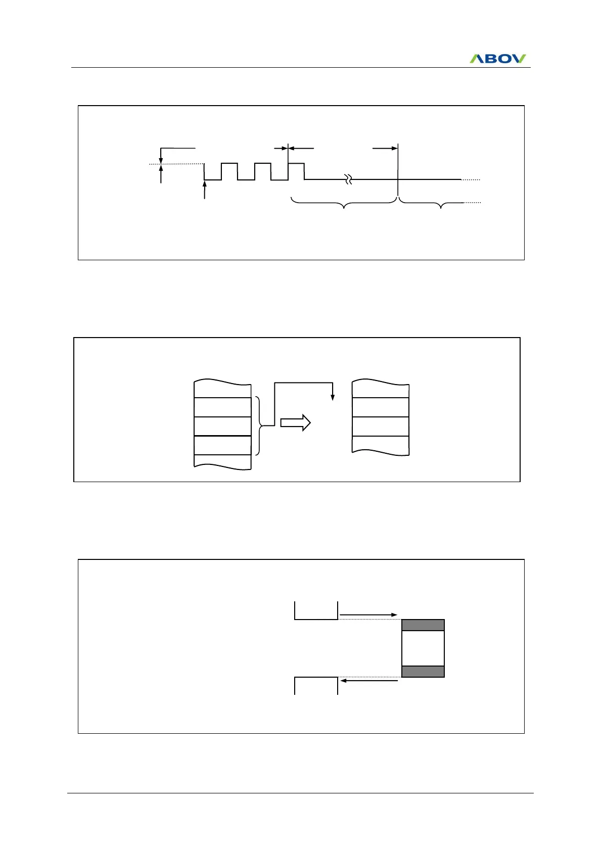
10.8 Interrupt Enable Accept Timing
Figure 10.7 Interrupt Response Timing Diagram
10.9 Interrupt Service Routine Address
Figure 10.8 Correspondence between Vector Table Address and the Entry Address of ISR
10.10 Saving/Restore General-Purpose Registers
Figure 10.9 Saving/Restore Process Diagram and Sample Source
INTxx : PUSH PSW
PUSH DPL
PUSH DPH
PUSH B
PUSH ACC
∙
∙
Interrupt_Processing:
∙
∙
POP ACC
POP B
POP DPH
POP DPL
POP PSW
RETI
Basic Interval Timer
Vector Table Address
Basic Interval Timer
Service Routine Address
Interrupt Processing
: LCALL & LJMP

 Loading...


