MC96F6432
110 June 22, 2018 Ver. 2.9
11. Peripheral Hardware
11.1 Clock Generator
11.1.1 Overview
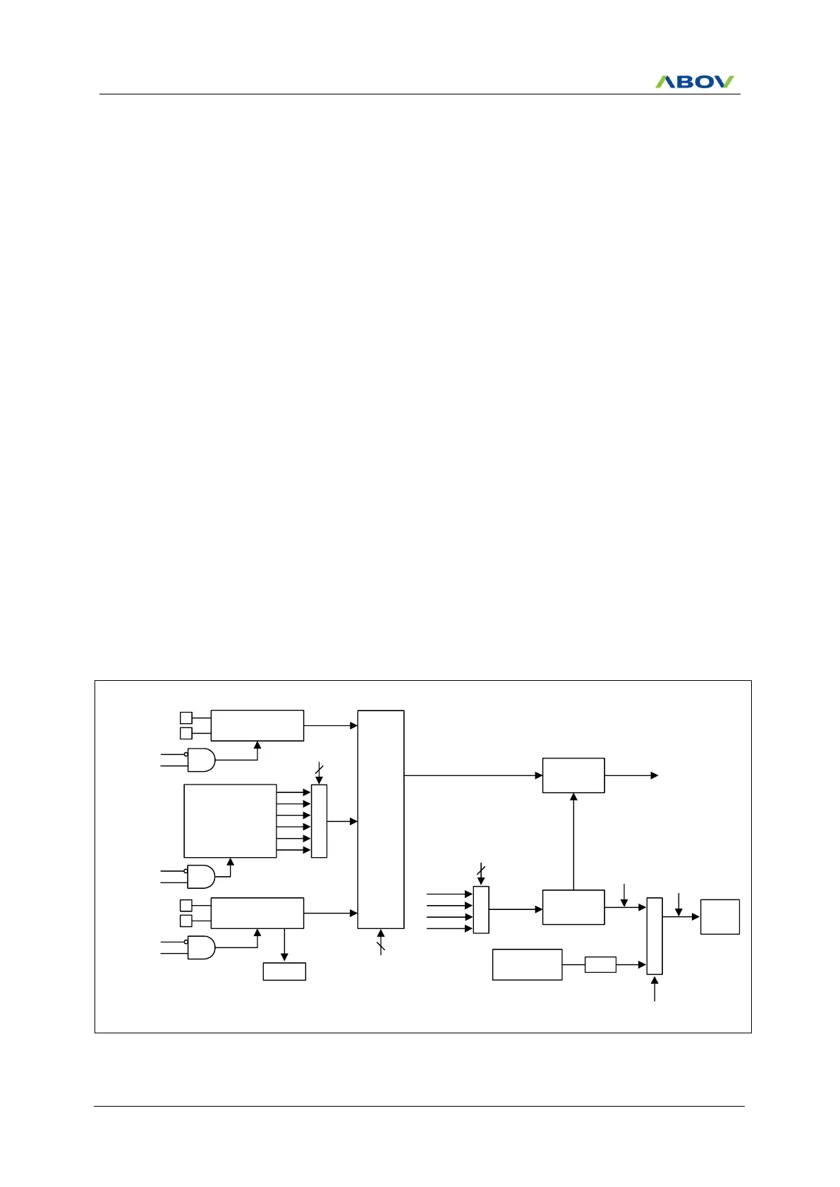
As shown in Figure 11.1, the clock generator produces the basic clock pulses which provide the system clock to
be supplied to the CPU and the peripheral hardware. It contains main/sub-frequency clock oscillator. The
main/sub clock operation can be easily obtained by attaching a crystal between the XIN/SXIN and XOUT/SXOUT
pin, respectively. The main/sub clock can be also obtained from the external oscillator. In this case, it is
necessary to put the external clock signal into the XIN/SXIN pin and open the XOUT/SXOUT pin. The default
system clock is 1MHz INT-RC Oscillator and the default division rate is eight. In order to stabilize system
internally, it is used 1MHz INT-RC oscillator on POR.
- Calibrated Internal RC Oscillator (16 MHz )
. INT-RC OSC/1 (16 MHz)
. INT-RC OSC/2 (8 MHz)
. INT-RC OSC/4 (4 MHz)
. INT-RC OSC/8 (2 MHz)
. INT-RC OSC/16 (1 MHz, Default system clock)
. INT-RC OSC/32 (0.5 MHz)
- Main Crystal Oscillator (0.4~12 MHz)
- Sub Crystal Oscillator (32.768 kHz)
- Internal WDTRC Oscillator (5 kHz)
11.1.2 Block Diagram
Clock
Change
System
Clock Gen.
(Core, System,
Peripheral)
BIT
WDT
BIT
overflow
XIN
XOUT
Main OSC
fXIN
STOP Mode
XCLKE
Internal RC OSC
(16MHz)
STOP Mode
IRCE
fIRC
1/1
1/2
1/4
1/8
M
U
X
WDTRC OSC
(5kHz)
WDTCK
Stabilization Time
Generation
M
U
X
BIT clock
WDT clock
SXIN
SXOUT
Sub OSC
fSUB
STOP Mode
SCLKE
WT
2
SCLK[1:0]
/256
1/16
1/32
3
IRCS[2:0]
fx/4096
fx/1024
fx/128
fx/16
M
U
X
2
BITCK[1:0]
SCLK
fx
Figure 11.1 Clock Generator Block Diagram

 Loading...


