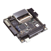
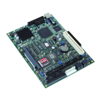
SBC-GX1 Technical Manual Detailed hardware description
I/O map
The PC/AT I/O address map is limited to 1K addresses. This is because only the lower
ten address lines were originally used to decode I/O devices. The remaining lines were
treated as undefined. Therefore the usable address range is from 0-3FFH. Above this
range, devices are imaged and accessed throughout the entire 64K I/O address range
of the processor.
The following table shows the I/O address mapping for the SBC-GX1. If expansion
boards are added via the PC/104 interface you should ensure that they are configured
to be at a free address location. Failure to do so will result in them not functioning
correctly, and may even cause the SBC-GX1 board to stop operating.
Device I/O location (hex)
DMA Controller 1 000-00F
Interrupt Controller 1 020-021
Timer/Counter 040-043
Keyboard/Mouse 060-064
Real Time Clock 070-071
DMA Page Registers 080-08F
Watchdog Timer 093
Interrupt Controller 2 0A0-0A1
DMA Controller 2 0C0-0DF
Audio 220-22F
Flash Paging Registers 258-259
RS232 Power-down Latch 260
COM4 2E8-2EF
COM2 2F8-2FF
MPU-401 330-33F
Parallel Port 378-37F (278-27F
1
)
Video Controller 3B0-3BB, 3C0-3CF, 3D0-3DF
COM3 3E8-3EF
Floppy Disk 3F0-3F7
COM1 3F8-3FF
The Parallel printer port is decoded at 378-37FH when using the Award BIOS,
and at 278-27FH when using the General Software BIOS.
© 2004 Arcom Issue D 67
 Loading...