e
e
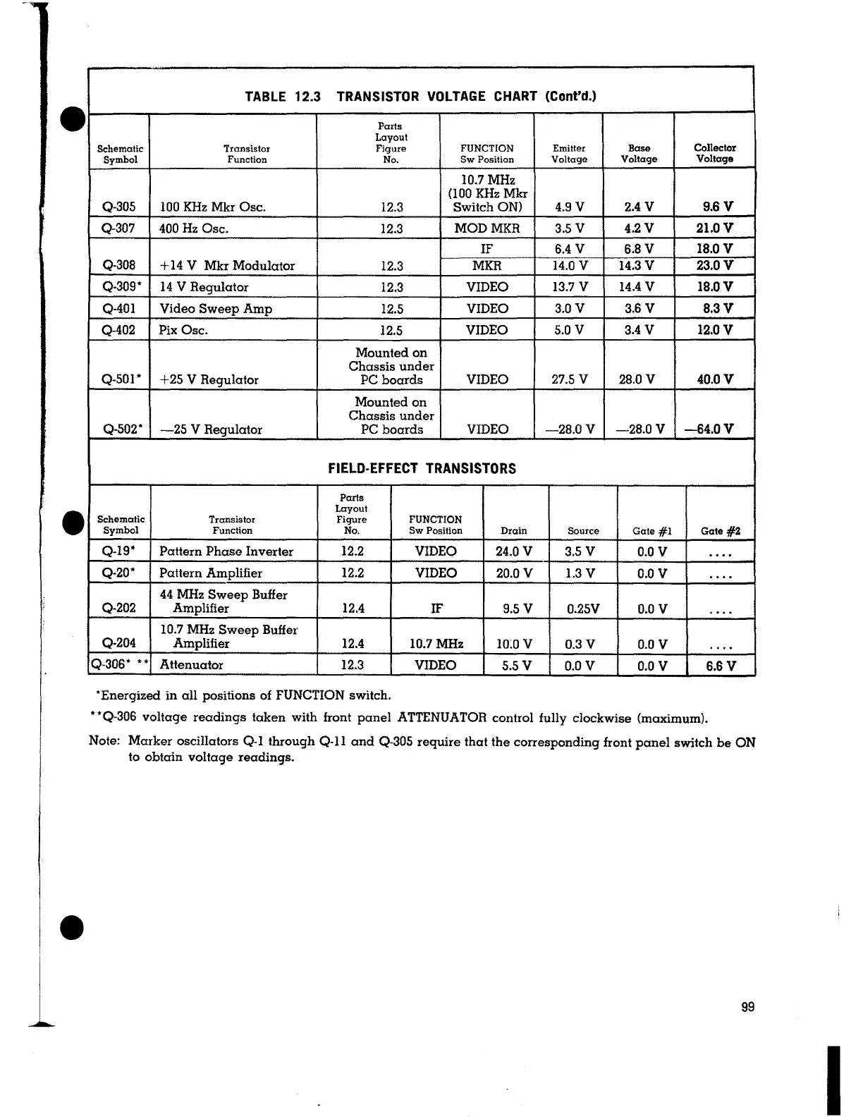
TABLE 12.3
TRANSISTOR VOLTAGE CHART (Cont'd.)
Parts
Layout
Schematic
Transistor Figure FUNCTION
Emitter
Base Collector
Symbol Function No. Sw Position
Voltage
Voltage
Voltage
10.7 MHz
(100 KHzMkr
Q-305
100 KHz Mkr Osc.
12.3
Switch ON)
4.9V
2.4 V
9.6V
Q-307
400 Hz Osc.
12.3
MODMKR
3.5 V 4.2V
21.0V
IF
6.4 V 6.8V
18.0V
Q-308
+14 V Mkr Modulator
12.3 MKR
14.0V
14.3 V
23.0V
Q-309*
14 V Regulator
12.3
VIDEO 13.7 V 14.4 V 18.0V
~eo Sweep Amp
12.5
VIDEO
3.0V 3.6V
8.3V
Osc.
12.5
VIDEO
5.0V 3.4 V
12.0V
Mounted on
Chassis under
Q-501
*
+25 V Regulator
PC hoards
VIDEO
27.5 V 28.0 V
40.0V
Mounted on
Chassis under
Q-502*
-25 V Regulator PC hoards VIDEO
-28.0V -28.0V
-64.0V
FIELD-EFFECT TRANSISTORS
Parts
Layout
Schematic Transistor Figure
FUNCTION
Symbol
Function No. Sw Position
Drain Source
Gate #1
Gate#2
Q-19*
Pattern Phase Inverter 12.2 VIDEO
24.0V 3.5V
o.ov ....
Q-20*
Pattern Amplifier 12.2
VIDEO
20.0V 1.3 V
o.ov
.....
44 MHz Sweep Buffer
Q-202
Amplifier
12.4
IF 9.SV
0.25V
o.ov ,. ....
Q-204
10.7 MHz Sweep Buffer
Amplifier
12.4 10.7 MHz
10:0V 0.3V
o.ov
....
Q-306* ••
Attenuator
12.3 VIDEO
5.5V
o.ov
o.ov
6.6V
*Energized in all positions of FUNCTION switch.
**Q-306 voltage readings taken with front panel ATTENUATOR control fully clockwise (maximum).
Note: Marker oscillators
Q-1 through Q-11 and Q-305 require that the corresponding front panel switch he ON
to obtain voltage readings.
99
I
 Loading...