THEORY
OF OPERATION
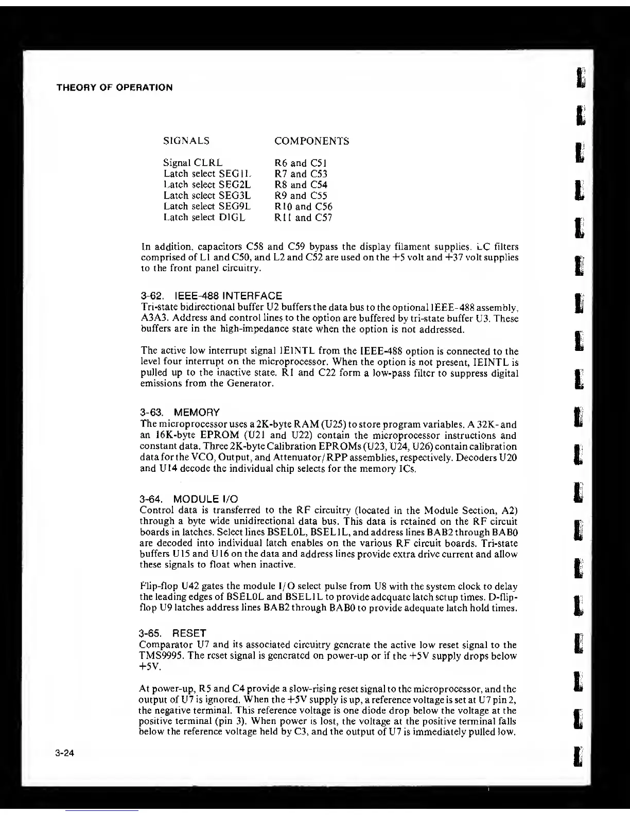
SIGNALS
Signal CLRL
Latch select
SEGIL
I.atch
select SEG2L
Latch select SEG3L
Latch select SEG9L
Latch select
DIGL
COMPONENTS
R6
and
C51
R7 and C53
R8 and C54
R9 and C55
RIO
and
C56
Rll and C57
In
addition, capacitors CSS and C59 bypass the display filament supplies.
LC
filters
comprised of LI and C50, and L2 and C52 are used on the
+5
volt and +37 volt supplies
to the front panel circuitry.
3-62.
IEEE-488 INTERFACE
Tri-stale bidirectional buffer U2 buffers the
data
bus to the optional IEEE- 488 assembly,
A3A3. Address and control lines to the
option
are buffered by tri-state buffer
U3.
These
buffers are in the high-impedance
state when the option
is not
addressed.
The active low interrupt signal lElNTL from
the IEEE-488 option is connected
to
the
level four interrupt on the
microprocessor.
When the option
is
not present, lEINTL is
pulled up to
the
inactive state. R1 and C22 form
a low-pass filter to suppress digital
emissions from the Generator.
3-63,
MEMORY
The
microprocessor
uses a 2K-byte RAM (U25) to store program variables. A
32K- and
an 16K-byte EPROM (U21 and
U22)
contain
the microprocessor instructions and
constant
data.
Three 2K-byte Calibration EPROMs (U23, U24, U26) contain calibration
data for the VCO, Output, and Attenuator/
RPP assemblies, respectively. Decoders U20
and
U
14
decode the individual chip selects for the memory
iCs,
3-64.
MODULE I/O
Control data is transferred to the RF circuitry
(located
in the Module Section, A2)
through a byte wide unidirectional
data
bus. This data is retained on the RF circuit
boards in latches. Select lines BSELOL, BSELIL, and address lines BAB2 through BABO
are decoded into individual latch enables on the
various
RF
circuit
boards. Tri-state
buffers U15 and UI6 on the data and
address lines
provide extra drive current and allow
these signals to float when inactive.
Flip-flop U42 gates the module I/O select pulse
from
U8 with the system clock to delay
the leading edges of BSELOL and BSELIL to provide
adequate latch setup times, D-flip-
flop U9 latches address lines BAB2 through
BABO to provide adequate latch hold times.
3-65.
RESET
Comparator
U7
and its
associated circuitry generate the active low reset signal to the
TMS9995. The reset signal is generated on power-up
or
if
the
+5V
supply drops below
+5V.
At
power-up, R5 and
C4
provide a
slow-rising
reset signal to the microprocessor, and the
output of U7
is
ignored. When
the
+5V
supply is up, a reference voltage is set at U7 pin
2,
the negative terminal. This reference voltage is one diode drop below the voltage at the
positive
terminal (pin
3).
When
power is lost, the voltage at the positive terminal falls
below the reference voltage held by C3, and the
output of U7 is
immediately
pulled low.
t
3-24