Theory of Operation
IEEE-488 INTERFACE
(OPTION
-05)-
signal. (A polarity selection procedure is given in the
Maintenance section.) The 8840A is configured in the
factory so that it is triggered on the falling edge of the
EXT TRIG signal.
5-42.
IEEE488
Interface Power Supply
The IEEE-488 Interface power supply circuit provides the
IEEE-488 Interface PCA with +5V. The circuit consists of
rectifying diodes CR908 and CR909, fiiter capacitor C910,
and voltage regulator VR901. Power comes from trans-
former T605 on the Main PCA. U'908 and associated
circuitry resets the Out-Guard
pC
at power-up and follow-
ing power-line voltage dropouts.
543.
TRUE
RMS
AC
(OPTION
-09)
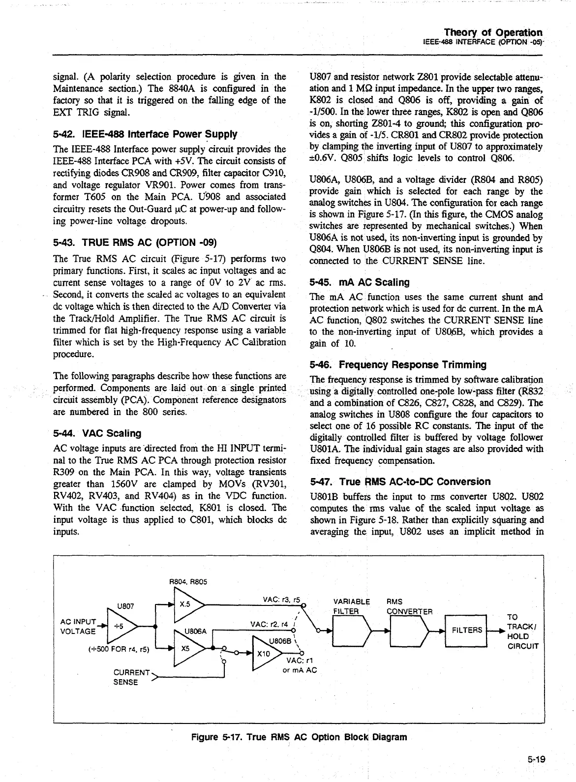
The True RMS AC circuit (Figure 5-17) performs two
primary functions. First, it scales ac input voltages and ac
current sense voltages to a range of OV to 2V ac rms.
Second, it converts the scaled ac voltages to
an
equivalent
dc
voltage which is then directed to the
AID
Converter via
the Track/Hold Amplifier. The
True
RMS AC circuit is
trimmed for flat high-frequency response using
a
variable
filter which is set by the High-Frequency AC Calibration
procedure.
The
following paragraphs describe how these functions
are
performed. Components are laid out on
a
single printed
circuit assembly (PCA). Component reference designators
are numbered in the 800 series.
5-44. VAC Scaling
AC voltage inputs are directed from the HI INPUT termi-
nal to the True RMS AC PCA through protection resistor
R309 on the Main PCA. In this way, voltage transients
greater than
1560V are clamped by MOVs (RV301,
RV402, RV403, and RV404)
as
in the VDC function.
With the VAC function selected, K801 is closed. The
input voltage is thus applied to
C801, which blocks dc
inputs.
U807 and resistor network 2801 provide selectable attenu-
ation and
1
MB input impedance. In the upper two
ranges,
K802 is closed and Q806
is
off, providing
a
gain of
-11500. In the lower three ranges, K802 is open and Q806
is on, shorting 2801-4 to ground; this configuration pro-
vides
a
gain of -115. CR801
and
CR802 provide protection
by clamping the inverting input of U807 to approximately
.-0.6V. Q805 shifts logic levels to control Q806.
U806A, U806B, and a voltage divider (R804 and R805)
provide gain which is selected for each range by the
analog switches in
U804.
The configuration for each
range
is shown in Figure 5-17. (In this figure, the CMOS analog
switches are represented by mechanical switches.) When
U806A
is not used, its non-inverting input is grounded by
Q804. When U806B is not used, its non-inverting input is
connected to the CURRENT SENSE line.
545.
mA AC Scaling
The
mA AC function uses the same current shunt and
protection network which is used for dc current. In the rnA
AC function, Q802 switches the CURRENT SENSE line
to the non-inverting input of U8WB, which provides a
gain of 10.
546.
Frequency Response Trimming
The frequency response is trimmed by software calibration
using a digitally controlled one-pole low-pass filter
(R832
and a combination of
C826,
C827, C828, and (3329). The
analog switches in U808 configure the four capacitors to
select one of 16 possible RC constants. The input of the
digitally controlled filter is buffered by voltage follower
U801A. The ihdividual gain stages are also provided with
fixed frequency compensation.
5-47. True RMS AC-to-DC Conversion
U801B buffers the input to
rms
converter U802. U802
computes the rms value of the sded input voltage
as
shown in Figure 5-18. Rather than explicitly squaring and
averaging the input, U802 uses an implicit method in
VARIABLE RMS
TO
FILTERS
HOLD
5
.I
CIRCUIT
Figure
5-17.
True
RMS
AC
Option Bioclc
Diagram
Artisan Technology Group - Quality Instrumentation ... Guaranteed | (888) 88-SOURCE | www.artisantg.com