monitored to indicate when the DAC output is larger than
This five-interval process thus generates five
ibbles
the input voltage.
which are processed by the In-Guard PC to produ e one
f
A,
sample. After the fifth nibble is generated, UlOl
conversion process is broken up id0 an aUtOZer0
intermpts the In-Guard
6
over line INT. The In&uard
pried
followed by five maurement intervals- (A timing
PC then pulls line
CS7
low five times, causing
~b01
to
diagram is shown in Figure 5-5.) Six bits of the
fid
A/D
~nd the
the five (six-bit) nHls onea-a-timb over
sample are obtained during each interval.
lines
ADO-ADS.
The In-Guard
wC
then weights each
nibble 1/16 of the value of the previous nu&& and
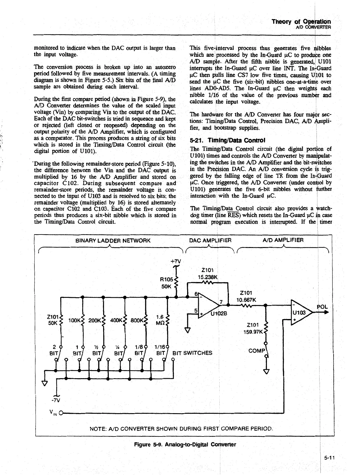
During the
first
compare period (shown in Figure
5-9),
the
the
input
voltage.
AID
Converter determines the value of the xaled inm
voltage (vin) by comparing Vin to the outpt of the
DAC.
he
harhare for the
AID
Convener has four maj r aec-
Each of the DAC bit-switches is tried in sequence and kept
tions:
~i~i~~~~~~~ c~~~~~~, hecision D~C,
bpli-
or rejected (left closed or reopned) depending on the
and
botrtrap
supplies.
output polarity of the
AD
Amplifier, which is configured
,
as
a COmparatOr.
This
process produces a string of six bits
5-21.
Tir(ling/g/D*
CoMml
which is stored in the TiminglData Control circuit (the
I
digital portion of U101).
The TimingIData Control circuit (the digital
U101) time and controls the
AlD
Converter by
'During the following remainder-store
period
(Figure 5-10),
the difference between the Vin and the DAC output is
multiplied by 16 by the
AD
Amplifier and stored on
capacitor C102. During subsequent compare and
remainder-store periods, the remainder voltage is con-
nected to the input of U103 and
is
resolved to six bits; the
remainder voltage (multiplied by 16) is stored alternately
on capacitor C102 and
C103. Each of the five compare
periods thus produces
a
six-bit nibble which is stored in
the TimingData Control circuit.
ing the swjtches in the
AD
Amplifier and thibit-ditches
in the Pre4ision DAC.
An
AD
conversion cycle
i
trig-
gered by the falling edge of line
TR
from the Inbuard
PC. Once triggered, the
AD
Converter (under conqrol by
U101) gerierates the five 6-bit nibbles without further
interaction with the In-Guard
PC.
,
The Timinoata Control circuit also provides a katch-
-
dog timer (line
RES)
which resets the In-Guard
pC
ib
case
normal program execution is interrupted. If the timer
I
BINARY LADDER
NETWORK
DAC
AMPLIF
IER
A/D
AMPLIFIER
Pr---7r------
R105
15.238K
50K
-7v
",N
0
.
NOTE: A/D CONVERTER SHOWN DURING FIRST COMPARE PERIOD.
Figure
5-9.
Analog-to-Digital Converter
Artisan Technology Group - Quality Instrumentation ... Guaranteed | (888) 88-SOURCE | www.artisantg.com