FC6A S
ERIES
MICROS
MART
L
ADDER
P
ROGRAMMING
M
ANUAL
FC9Y-B1726 5-13
5: M
OVE
I
NSTRUCTIONS
Repeat Operation in the Indirect Bit Move Instructions
Repeat Bit Devices (Source and Destination)
If a repeat operation is set for bit devices such as input, output, internal relay, or shift register, as many bit devices as the repeat
cycles are moved.
Repeat Word Devices (Source and Destination)
If a repeat operation is for word devices such as data register, as many bit devices as the repeat cycles in the designated data
register are moved.
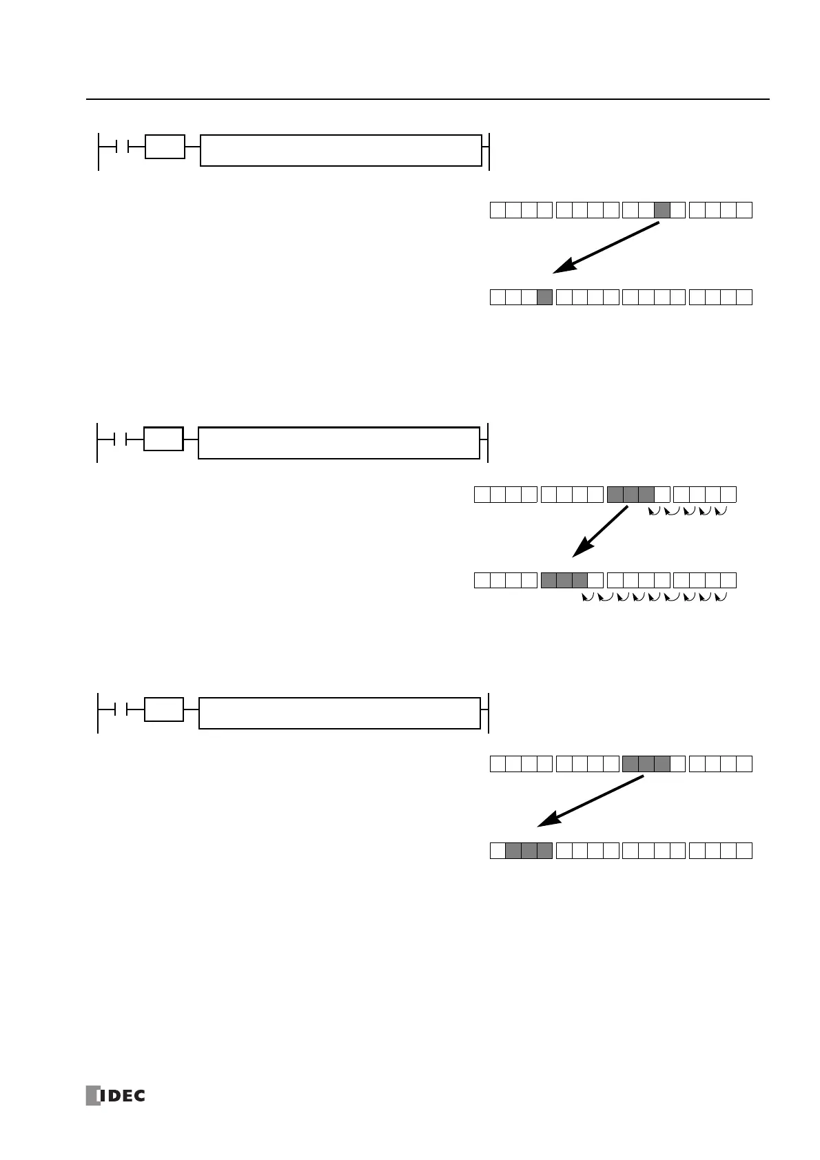
D10 + 5 → D20 + 12
Since source device S1 is a data register and the value of source device
S2 is 5, the source data is bit 5 of data register D10 assigned by source
device S1.
Since destination device D1 is a data register and the value of source
device D2 is 12, the destination is bit 12 of data register D20 assigned by
destination device D1.
As a result, when input I0 is on, the ON/OFF status of data register D10
bit 5 is moved to data register D20 bit 12.
S1 –
D10
I0
IBMV S2
5
D1 –
D20
SOTU
REPD2
12
Bit 15
Bit 5
Bit 12
14 13 12 11 10 9 8 7654 3210
D10
Bit 15 14 13 12 11 10 9 8 7654 3210
D20
M10 + 5 → Q0 + 9
Repeat = 3
Since source device S1 is internal relay M10 and the value of source
device S2 is 5, the source data is 3 internal relays starting with M15.
Since destination device D1 is output Q0 and the value of destination
device D2 is 9, the destination is 3 outputs starting with Q11.
As a result, when input I1 is on, the ON/OFF statuses of internal relays
M15 through M17 are moved to outputs Q11 through Q13.
S1 R
M10
I1
IBMV S2
5
D1 R
Q0
SOTU
REP
3
D2
9
M27 M10M17M20 M15
5th from M10
Q17 Q0Q7Q11
9th from Q0
Q14 Q13
D10 + 5 → D20 + 12
Repeat = 3
Since source device S1 is data register D10 and the value of source
device S2 is 5, the source data is 3 bits starting with bit 5 of data register
D10.
Since destination device D1 is data register D20 and the value of
destination device D2 is 12, the destination is 3 bits starting with bit 12 of
data register D20.
As a result, when input I2 is on, the ON/OFF statuses of data register D10
bits 5 through 7 are moved to data register D20 bits 12 through 14.
S1 R
D10
I2
IBMV S2
5
D1 R
D20
SOTU
REP
3
D2
12
Bit 15
Bit 5
Bit 12
14 13 12 11 10 9 8 7654 3210
D10
Bit 15 14 13 12 11 10 9 8 7654 3210
D20
 Loading...