10: D
ATA
C
ONVERSION
I
NSTRUCTIONS
10-16 FC6A S
ERIES
MICROS
MART
L
ADDER
P
ROGRAMMING
M
ANUAL
FC9Y-B1726
DECO (Decode)
Valid Devices
For valid device address ranges, see "Device Addresses" on page 2-1.
Special internal relays cannot be designated as D1.
Valid values for the offset designated by source device S1 are 0 through 255. Make sure that the offset designated by S1 and the last bit of
destination data determined by the sum of S1 and D1 are within the valid value range. If the offset or destination data exceeds the valid range, a
user program execution error will result, turning on special internal relay M8004 and the ERR LED on the FC6A Series MICROSmart.
When a user program execution error occurs, the execution of the instruction is canceled. The value of D1 is left unchanged and the next instruction
is executed. For user program execution errors, see "User Program Execution Errors" on page 3-10.
Since the DECO instruction is executed in each scan while input is on, a pulse input from a SOTU or SOTD instruction should be used.
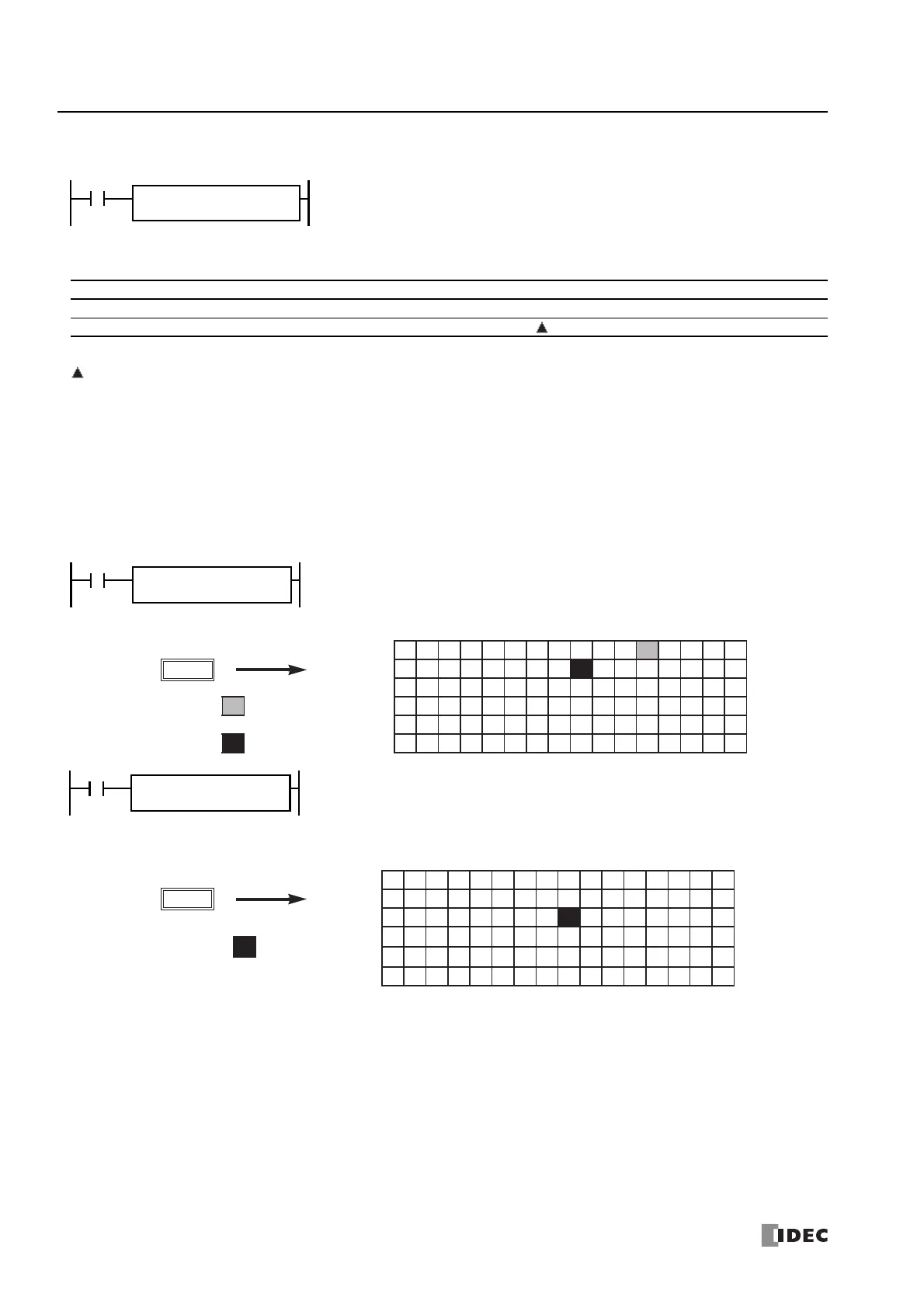
Examples: DECO
When input is on, the values contained in devices assigned by S1 and D1 are added together to
determine the destination, and the bit is then turned on.
Device Function I Q M R T C D P Constant Repeat
S1 (Source 1) Offset XXXX——X— X —
D1 (Destination 1) First bit to count offset — X X — — X — — —
When input I0 is on, the destination bit is determined by adding the value contained in data
register D20 assigned by device S1 to internal relay M104 assigned by destination device D1.
Since the 19th bit from internal relay M104 is internal relay M127, the bit is then turned on.
M117 M100
M137
M120
M157 M140
First bit M177 M160
M197 M180
ON M217 M200
19
D20
When input I1 is on, the destination bit is determined by adding the value contained in data
register D10 assigned by device S1 to data register D30 assigned by destination device D1.
Since the 39th bit from data register D30 bit 0 is data register D32 bit 7, the bit is then turned
on.
Bit 1514131211109876543210
D30
D31
D32
D33
ON
D34
D35
39
D10
 Loading...