Theory Of Operation: Major Assemblies 2-5
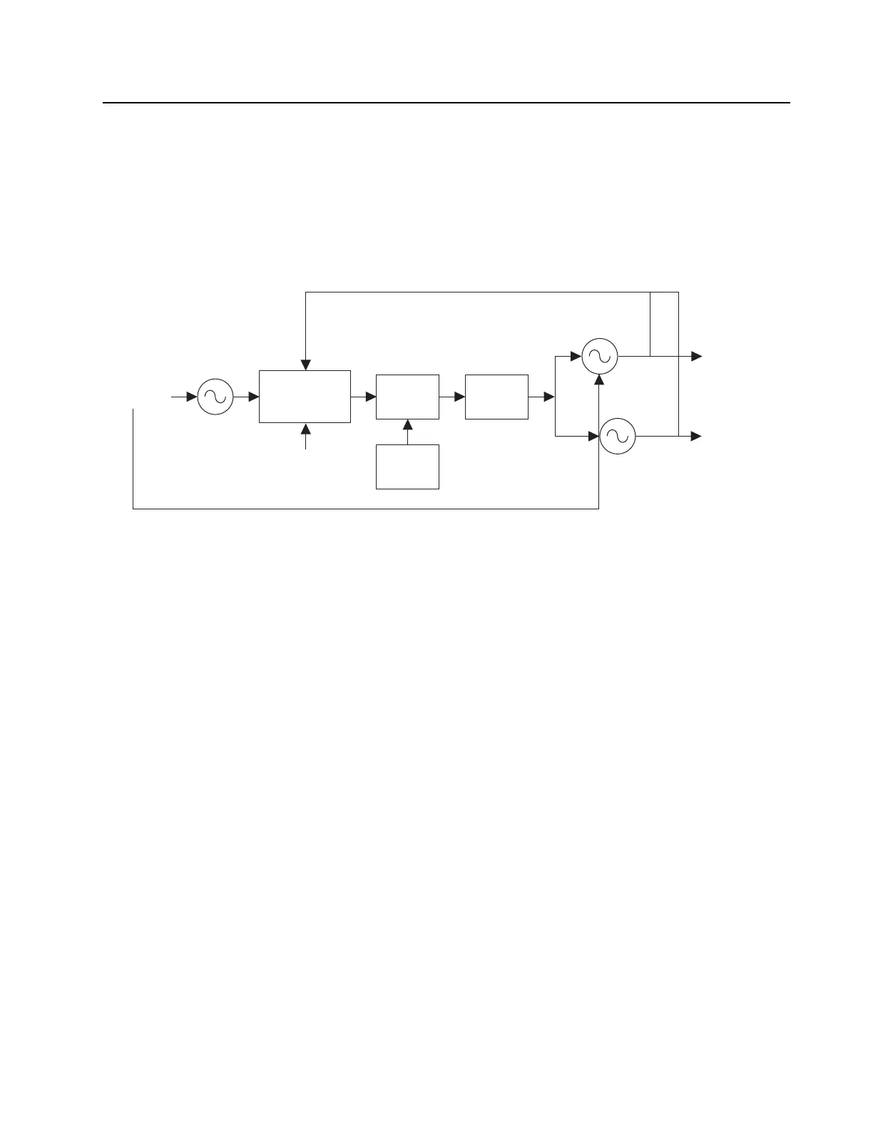
2.2.3 Phase Lock Loop Synthesizer
The Phase Lock Loop (PLL) synthesizer subsystem consists of the reference oscillator (VCTCXO),
VCO, PLL IC, Charge pump and Loop filter.
VCTCXO (Voltage Controlled Temperature Compensated crystal Oscillator) reference frequency
(12.8 MHz) provides reference to PLL IC, with stability of +/-2.5PPM at -30° to +60°C. This reference
frequency is divided to 6.25 kHz or 5 kHz by PLL IC. PLL IC outputs 2 Signals (P & R) depending on
phase difference. A charge pump is used to charge these output signals from 0 – 3.3 V up to
0 – 10 V which is required to control the VCO. A voltage doubler (U507) converts 5 V to 10 V to
supply the necessary voltage for a higher frequency resolution in VCO. The Loop filter is a Low Pass
filter (C751 – C754, R726 – R728) to reduce the residual side-band noise of VCO Reference
Frequency for the best signal-to-noise ratio. The VCO module contains both RX VCO and TX VCO,
configured as Collpits oscillators and connects to DC power through cascaded buffers. Q705 and
Q305 enable RX VCO when RX_EN is high. Q706 and Q503 enable TX VCO when TX_EN1 is high.
The input audio signal for TX VCO is from (U501-B) and applied to a varactor diodes (CR703) in
TX VCO to be modulated into TX RF signal.
Figure 2-3. PLL Synthesizer Block Diagram
Modulating
Signal
FL701
12.8MHz
Ref.OSC.
Charge
Pump
Loop
Filter
TX VCO
RX Out
To Mixer
To PA Drive
TX Out
Circuit
RX VCO
Circuit
Voltage
Doubler
Synthesizer
U701
PLL Data
from μP

 Loading...