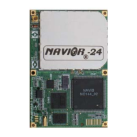
AVIOR-24S ™ CHAPTER II
Hardware Integration
34
NAVIOR-24S ™ Revision V1.00 20.05.2008
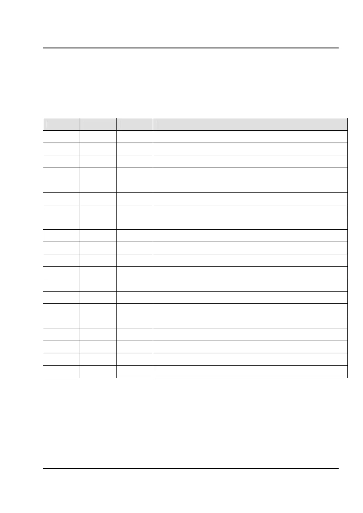
Digital IO/Power Connector Pin out
The digital IO/Power connector pin out information is listed in Table II-2.
Table II-2 - X501 I/O Connector Signals
Pin Name Direction Description
1 VCC Input
Prime Power (VCC)
2 GND -
Ground signals and power
3 VCC Input
Prime Power (VCC)
4 GND -
Ground signals and power
5 1PPS Output
Pulse-Per-Second, 3.3 V TTL CMOS
6 S_IN -
Technological pin - do not connect
7 TXDA Output
Serial port A transmit, 3.3V TTL CMOS
8 HS_OUT -
Technological pin - do not connect
9 TXDB Output
Serial port B transmit, 3.3V TTL CMOS
10 RXDA Input
Serial Port A receive, 3.3 V TTL CMOS
11 Р3 -
Reserved pin - do not connect
12 RXDB Input
Serial Port B receive, 3.3 V TTL CMOS
13 Р5 -
Reserved pin - do not connect
14 Р4 -
Reserved pin - do not connect
15 STATUS Output
Indicate work status
16 NC -
Reserved pin - do not connect
17 RES Input
External reset. Active level low
18 NC -
Reserved pin - do not connect
19 BBP Input
Battery Backup Power (+3 V DC)
20 VANT Input
Antenna power (+3…+5 V DC)
Note - If the pin is not in use, let it be not connected.