NSW-5
System Module UT5U
PAMS Technical Documentation
Page 44
Issue 1 10/00
Nokia Mobile Phones Ltd.
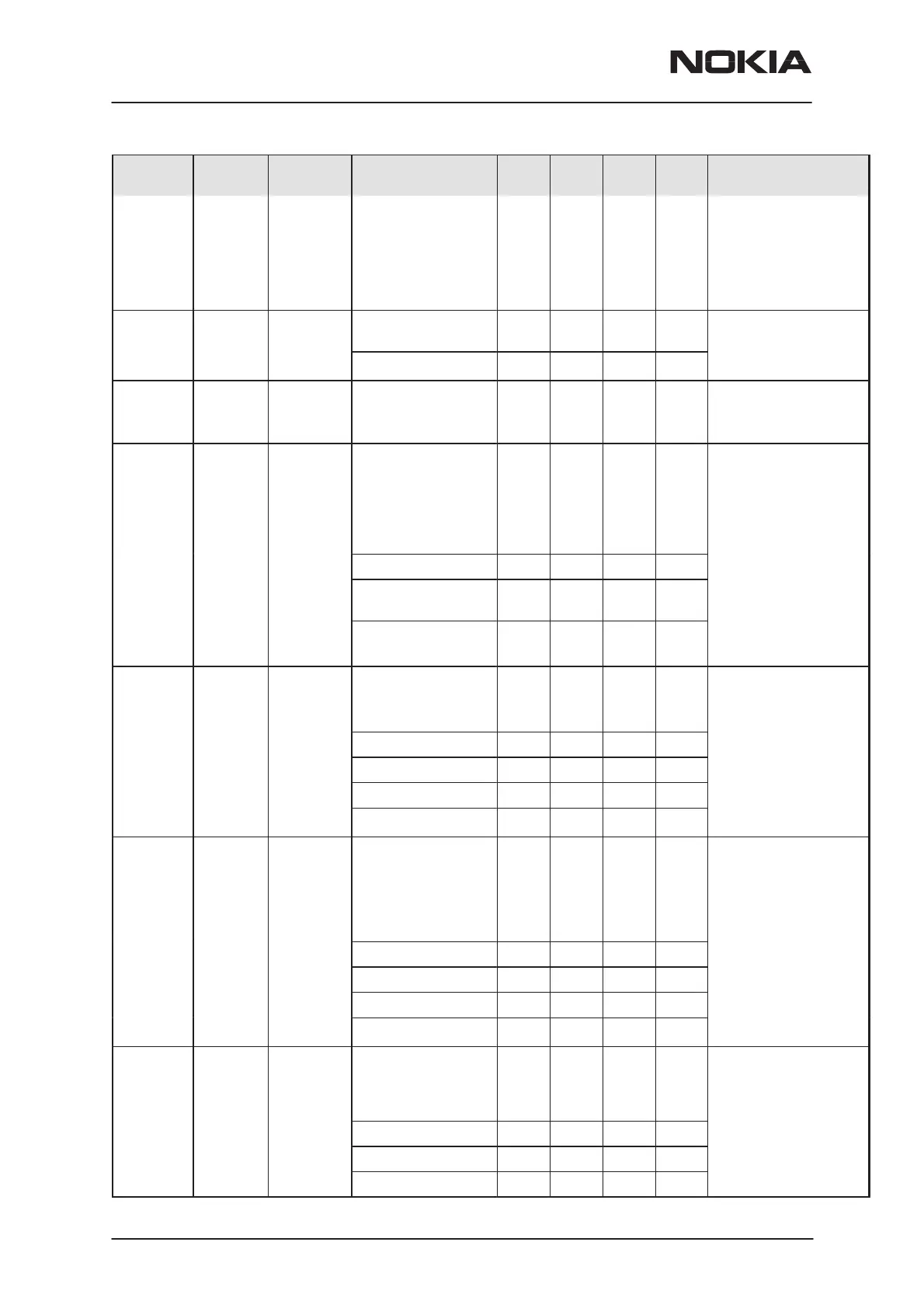
FunctionUnitMaxTypMinParameterToFrom/
Control
Signal
name
VR7_bias CCONT
/
VMODE
RF
800MhZ
PA bias
control for
analog
mode
Logic high ”1” tbd V 800MHz PA bias volt-
age is increased to
improve analog mode
efficiency
V5V CCONT
/
EROTUS
Voltage 4.8 5.0 5.2 V Erotus and discrete
synthesizer phase det
RFCEN
Current 3.0 5.0 mA
RFTEMP RF CCONT Voltage 0 1.5 V RF temperature sen-
sor (47 k NTC to
GND)
AFC Cob-
ba_D
VCTCXO
Voltage Min 0.05 1.2 2.25 V Automatic frequency
control signal for
VCTCXO. When
DAC is switched
OFF AFC output is in
high–Z mode
Resolution 11 bits
Load resistance
(dynamic)
10 kΩ
Load resistance
(DC)
110 kΩ
AGC1 Cob-
ba_D
EROTUS
Voltage Min 0.7 1.40 V Digital mode receiver
gain control.
DSP
Load resistance 10 kΩ
Load capacitance 10 pF
Resolution 10 bits
Timing inaccuracy 8 us
AGC2 MAD
(CTID
AGC2,
genpio)
RX LNA
Logic high ”1” 2.0 V LNA gain switch.
Polarity: 0=reduced
1=normal
DSP
Logic low ”0” 0.5 V
Sink/source curr. 10 100 uA
Load capacitance 10 pF
Timing inaccuracy 8 us
IF2AP/
IF2AN
ERO-
TUS
Cobba_D
IF2 frequency 450 kHz Differential IF2–sig-
nal from limiter to
DEMO detector in
Cobba_D
Output level, 0.2 Vpp
Load resistance 10 kΩ
Load capacitance 5 pF
 Loading...