MS51
Nov. 28, 2019 Page 25 of 491 Rev 1.00
MS51 32K SERIES TECHNICAL REFERENCE MANUAL
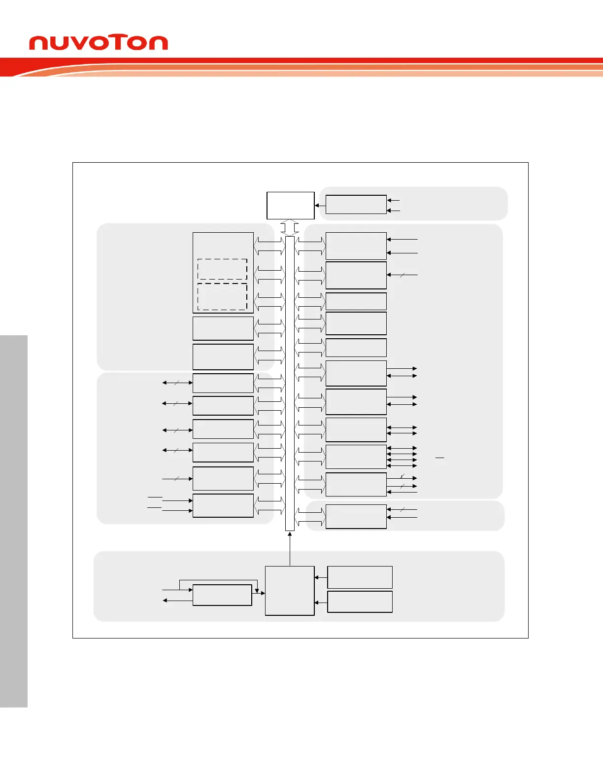
5 BLOCK DIAGRAM
5.1 MS51 32K Series Block Diagram
Figure 5.1-1 Functional Block Diagram shows the MS51 functional block diagram and gives the outline
of the device. User can find all the peripheral functions of the device in the diagram.
1T High
Performance
8051 Core
PWM0/1/2/3
Watchdog Timer
Serial Ports
(UART 0/1)
Timer 0/1
POR / LVR / BOD
I
2
C0
I2C0_SDA
I2C0_SCL
V
DD
V
SS
Timer 2
with
Input Capture
FB0
SPI0
12-bit ADC
15
Self Wake-up
Timer
Timer 3
UART2/3/4
(ISO 7816-3 port)
8-bit Internal Bus
AIN0~7, 9~15
STADC
UART2/3/4_TX
UART2/3/4_RX
UART0/1_RX
UART0/1_TX
SPI0_MOSI
SPI0_SS
SPI0_SCK
SPI0_MISO
ICAP0~2
T1
T0
6
3
32 KB APROM
Flash
Max. 4KB
LDROM Flash
Max. Bytes
Data Flash
(page: 128B)
Clock Divider
16/24 MHz Internal
RC Oscillator
(HIRC)
System Clock
4-24 MHz
Oscillator Circuit
(HXT)
XIN
XOUT
256 bytes
Internal RAM
P1
P2
P3
P1[7:0]
8
8
P3[7:0]
P0
P0[7:0]
8
P2[5:0]
6
Any Port
8
GPIO Interrupt
External Interrupt
INT0
INT1
2 Kbytes XRAM
(Auxiliary RAM)
PWM0CH0~5
Memory
Access
GPIO
Analog
Peripheral
System Clock
Source
Digital
Peripheral
Power
Management
6
PWM1/2/3CH0~1
10 kHz Internal RC
Oscillator
(LIRC)
Figure 5.1-1 Functional Block Diagram