MS51
Nov. 28, 2019 Page 429 of 491 Rev 1.00
MS51 32K SERIES TECHNICAL REFERENCE MANUAL
6.12 Serial Peripheral Interface (SPI)
6.12.1 Overview
The MS51 provides two Serial Peripheral Interface (SPI) block to support high-speed serial
communication. SPI is a full-duplex, high-speed, synchronous communication bus between
microcontrollers or other peripheral devices such as serial EEPROM, LCD driver, or D/A converter. It
provides either Master or Slave mode, high-speed rate up to F
SYS
/2, transfer complete and write
collision flag. For a multi-master system, SPI supports Master Mode Fault to protect a multi-master
conflict.
Divider
/2, /4, /8, /16
Select
MSB LSB
Pin Contorl Logic
MISO
MOSI
SPCLK
SS
SPI Status Control Logic
SPI Status Register SPI Control Register
Clock Logic
S
M
M
S
CLOCK
SPIF
WCOL
SPIOVF
MODF
DISMODF
SPI Interrupt
SPIEN
MSTR
MSTR
SSOE
DISMODF
SPR0
SPR1
SPR0
SPR1
CPHA
CPOL
MSTR
LSBFE
SPIEN
SSOE
SPIEN
Internal
Data Bus
F
SYS
Write Data Buffer
8-bit Shift Register
Read Data Buffer
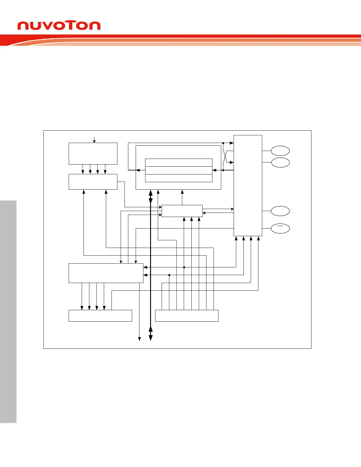
Figure 6.12-1 SPI Block Diagram
Figure15.1 SPI Block Diagram shows SPI block diagram. It provides an overview of SPI architecture in
this device. The main blocks of SPI are the SPI control register logic, SPI status logic, clock rate
control logic, and pin control logic. For a serial data transfer or receiving, The SPI block exists a write
data buffer, a shift out register and a read data buffer. It is double buffered in the receiving and
transmit directions. Transmit data can be written to the shifter until when the previous transfer is not
complete. Receiving logic consists of parallel read data buffer so the shift register is free to accept a
second data, as the first received data will be transferred to the read data buffer.
The four pins of SPI interface are Master-In/Slave-Out (MISO), Master-Out/Slave-In (MOSI), Shift
Clock (SPCLK), and Slave Select (SS
). The MOSI pin is used to transfer a 8-bit data in series from the
Master to the Slave. Therefore, MOSI is an output pin for Master device and an input for Slave.