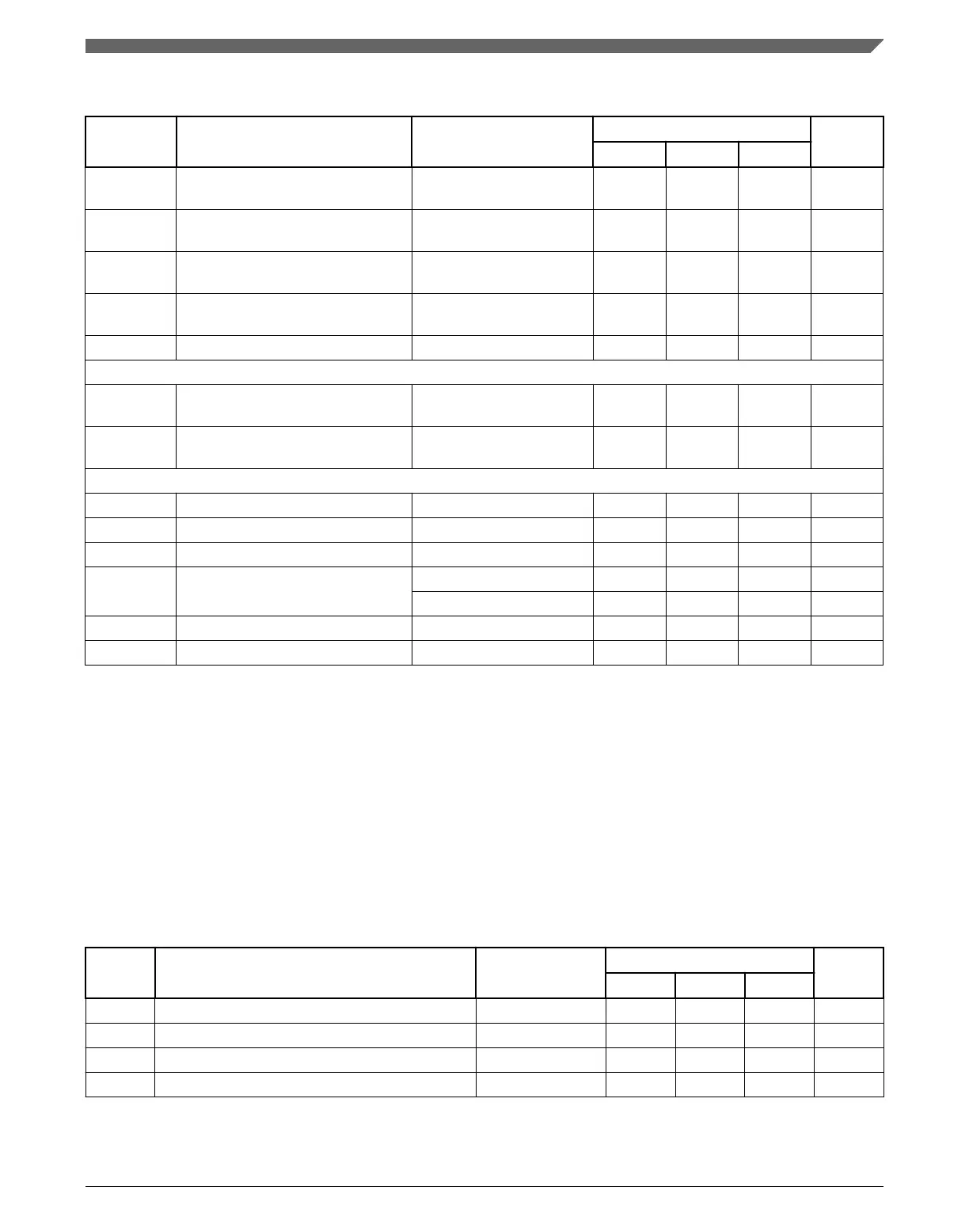
Table 22. LVDS pad startup and receiver electrical characteristics
Symbol Parameter Conditions
Value
Unit
Min Typ Max
t
PD2NM_TX
Transmitter startup time (power
down to normal mode)
1
—
— 0.4 0.55 µs
t
SM2NM_TX
Transmitter startup time (sleep
mode to normal mode)
2
Not applicable to the MSC/
DSPI LVDS pad
— 0.2 0.5 µs
t
PD2NM_RX
Receiver startup time (power down
to normal mode)
3
—
— 20 40 ns
t
PD2SM_RX
Receiver startup time (power down
to sleep mode)
4
Not applicable to the MSC/
DSPI LVDS pad
— 20 50 ns
I
LVDS_BIAS
LVDS bias current consumption Tx or Rx enabled — — 0.95 mA
TRANSMISSION LINE CHARACTERISTICS (PCB Track)
Z
0
Transmission line characteristic
impedance
—
47.5 50 52.5 Ω
Z
DIFF
Transmission line differential
impedance
—
95 100 105 Ω
RECEIVER
V
ICOM
Common mode voltage — 0.15
5
— 1.6
6
V
|Δ
VI
| Differential input voltage — 100 — — mV
V
HYS
Input hysteresis — 25 — — mV
R
IN
Terminating resistance V
DD_HV_IO
= 5.0 V ± 10% 80 100 120 Ω
V
DD_HV_IO
= 3.3 V ± 10% 80 115 150 Ω
C
IN
Differential input capacitance
7
— — 3.5 6.0 pF
I
LVDS_RX
Receiver DC current consumption Enabled — — 0.5 mA
1. Total transmitter startup time from power down to normal mode is t
STRT_BIAS
+ t
PD2NM_TX
+ 2 peripheral bridge clock
periods. The LFAST and High-Speed Debug LFAST pad electrical characteristics are based on worst case internal
capacitance values.
2. Total transmitter startup time from sleep mode to normal mode is t
SM2NM_TX
+ 2 peripheral bridge clock periods. Bias block
remains enabled in sleep mode. All LFAST and High-Speed Debug LVDS pad electrical characteristics are valid from -40
°C to 150 °C.
3. Total receiver startup time from power down to normal mode is t
STRT_BIAS
+ t
PD2NM_RX
+ 2 peripheral bridge clock periods.
4. Total receiver startup time from power down to sleep mode is t
PD2SM_RX
+ 2 peripheral bridge clock periods. Bias block
remains enabled in sleep mode.
5. Absolute min = 0.15 V – (285 mV/2) = 0 V
6. Absolute max = 1.6 V + (285 mV/2) = 1.743 V
7. Total internal capacitance including receiver and termination, co-bonded GPIO pads, and package contributions.
Table 23. LFAST transmitter electrical characteristics
Symbol Parameter Conditions
Value
Unit
Min Typ Max
f
DATA
Data rate — — — 320 Mbps
V
OS
Common mode voltage — 1.08 — 1.32 V
|V
OD
| Differential output voltage swing (terminated)
1, 2
— 100 200 285 mV
t
TR
Rise/Fall time (10%–90% of swing)
3, 4
— 0.26 — 1.5 ns
Table continues on the next page...
LVDS fast asynchronous serial transmission (LFAST) pad electrical characteristics
SPC5746R Microcontroller Data Sheet, Rev. 6, 06/2017
NXP Semiconductors 43

 Loading...


