Table 35. JTAG pin AC electrical characteristics (continued)
# Symbol Characteristic
Value
Unit
Min Max
7 t
TDOI
TCK low to TDO data invalid 0 — ns
8 t
TDOHZ
TCK low to TDO high impedance — 15 ns
9 t
JCMPPW
JCOMP assertion time 100 — ns
10 t
JCMPS
JCOMP setup time to TCK low 40 — ns
11 t
BSDV
TCK falling edge to output valid — 600
2
ns
12 t
BSDVZ
TCK falling edge to output valid out of high impedance — 600 ns
13 t
BSDHZ
TCK falling edge to output high impedance — 600 ns
14 t
BSDST
Boundary scan input valid to TCK rising edge 15 — ns
15 t
BSDHT
TCK rising edge to boundary scan input invalid 15 — ns
1. Timing includes TCK pad delay, clock tree delay, logic delay and TDO output pad delay.
2. Applies to all pins, limited by pad slew rate. Refer to IO delay and transition specification and add 20 ns for JTAG delay.
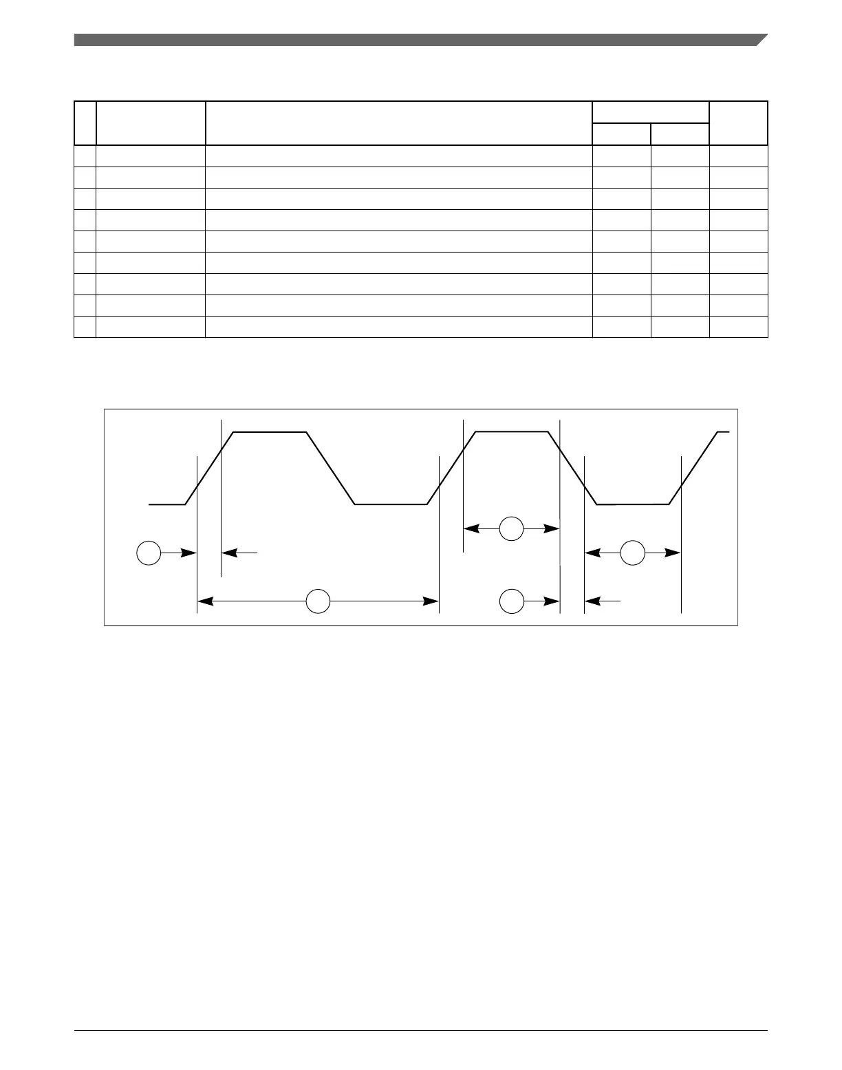
Figure 22. JTAG test clock input timing
AC specifications
SPC5746R Microcontroller Data Sheet, Rev. 6, 06/2017
NXP Semiconductors 59

 Loading...


