MPC5777M Microcontroller Data Sheet, Rev. 6
Electrical characteristics
NXP Semiconductors106
2t
CSV
CC PCS valid after SCK
5
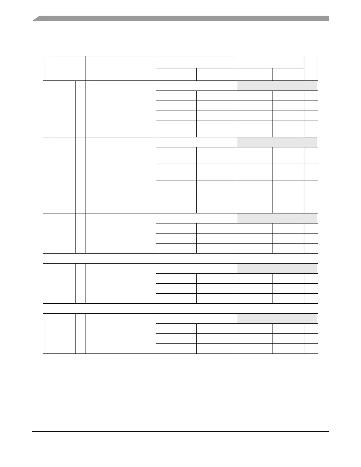
SCK and PCS drive strength
Very strong 25 pF 7 —ns
Strong 50 pF 8 —ns
Medium 50 pF 16 —ns
PCS medium
and SCK strong
PCS = 50 pF
SCK = 50 pF
29 —ns
3t
CSH
CC PCS hold after SCK
5
SCK and PCS drive strength
Very strong PCS = 0 pF
SCK = 50 pF
–14 —ns
Strong PCS = 0 pF
SCK = 50 pF
–14 —ns
Medium PCS = 0 pF
SCK = 50 pF
–33 —ns
PCS medium
and SCK strong
PCS = 0 pF
SCK = 50 pF
–35 —ns
4t
SDC
CC SCK duty cycle
6
SCK drive strength
Very strong 0pF
1
/
2
t
SCK
–2
1
/
2
t
SCK
+2 ns
Strong 0pF
1
/
2
t
SCK
–2
1
/
2
t
SCK
+2 ns
Medium 0pF
1
/
2
t
SCK
–5
1
/
2
t
SCK
+5 ns
SOUT data valid time (after SCK edge)
9t
SUO
CC SOUT data valid time from
SCK
CPHA = 1
7
SOUT and SCK drive strength
Very strong 25 pF — 7.0 ns
Strong 50 pF — 8.0 ns
Medium 50 pF — 16.0 ns
SOUT data hold time (after SCK edge)
10 t
HO
CC SOUT data hold time after
SCK
CPHA = 1
7
SOUT and SCK drive strength
Very strong 25 pF –7.7 — ns
Strong 50 pF –11.0 — ns
Medium 50 pF –15.0 — ns
1
TSB = 1 or ITSB = 1 automatically selects MTFE = 1 and CPHA = 1.
2
All output timing is worst case and includes the mismatching of rise and fall times of the output pads.
3
All timing values for output signals in this table are measured to 50% of the output voltage.
4
Timing is guaranteed to same drive capabilities for all signals, mixing of pad drives may reduce operating speeds
and may cause incorrect operation.
5
With TSB mode or Continuous SCK clock mode selected, PCS and SCK are driven by the same edge of
DSPI_CLKn. This timing value is due to pad delays and signal propagation delays.
Table 56. DSPI CMOS master timing – output only – timed serial bus mode TSB = 1 or ITSB = 1, CPOL = 0 or
1, continuous SCK clock
1,2
(continued)
# Symbol Characteristic
Condition Value
3
Unit
Pad drive
4
Load (C
L
)Min Max

 Loading...


