NXP Semiconductors
AN13134
PN76 family evaluation board quick start guide
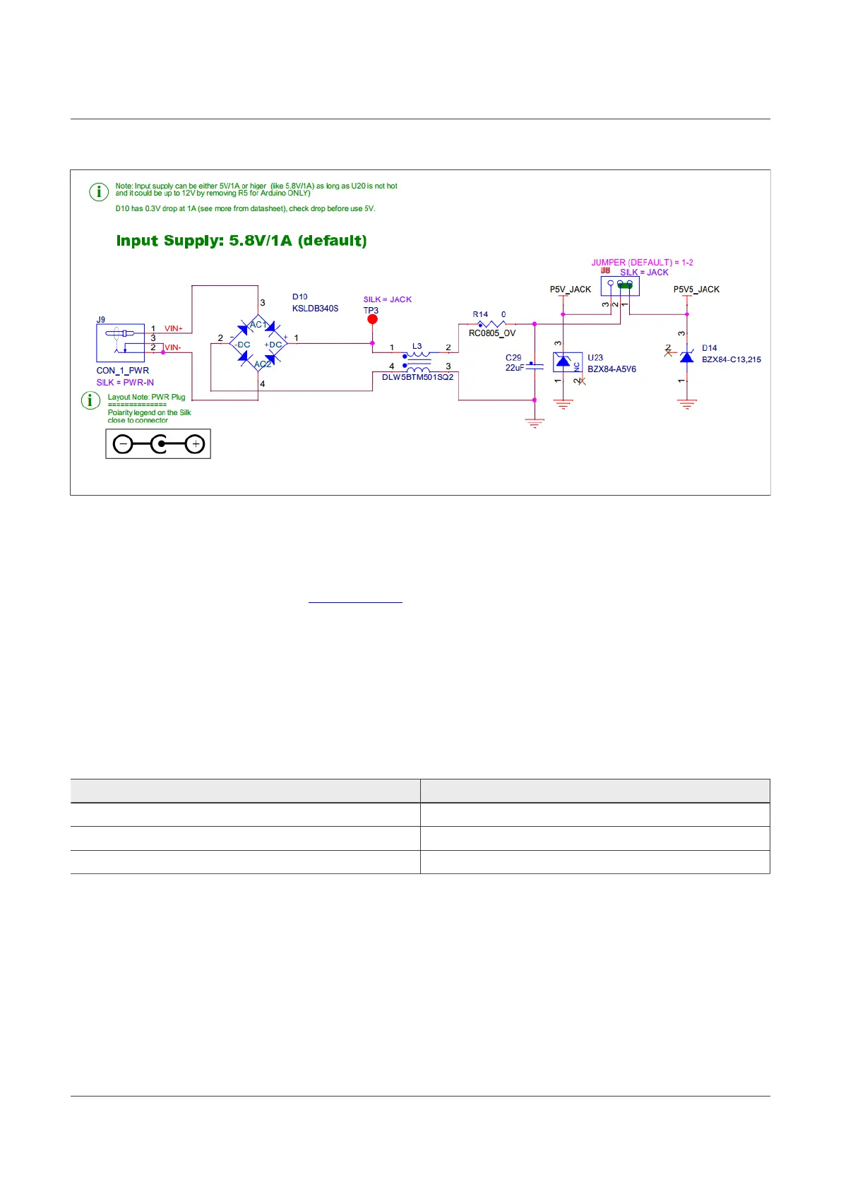
Figure 8. PNEV76FAMA power jack schematic
2.1.2 Debug interfaces
The board offers two ways of debugging. They are mutual exclusive. Hardware changes have to be made to
switch from one to the other.
Per default, the JTAG/SWD interface (Section 2.1.2.1) for an external debugger is active.
2.1.2.1 JTAG/SWD interface
The PN76 controller can be programmed via an SWD interface which is exposed as J21 "NFC-Debug" on the
PNEV7642A board. To access the SWD interface, J17 has to be set to 2-3 (default).
The current SDK is built to use a SEGGER J-Link, MCU-Link, or a LPC-Link2. Those external debuggers are
connected to J21 with a ribbon cable. In case you use a SEGGER J-Link make sure to have installed the latest
SDK (>V7.84).
Pins connected Description
1-2 JTAG Interface
2-3 SWD Interface (recommended)
3-4 JTAG Interface
Table 7. J17 Interface jumper setting
AN13134 All information provided in this document is subject to legal disclaimers. © 2023 NXP B.V. All rights reserved.
Application note Rev. 2.5 — 2 May 2023
11 / 57

 Loading...


