NXP Semiconductors
AN13134
PN76 family evaluation board quick start guide
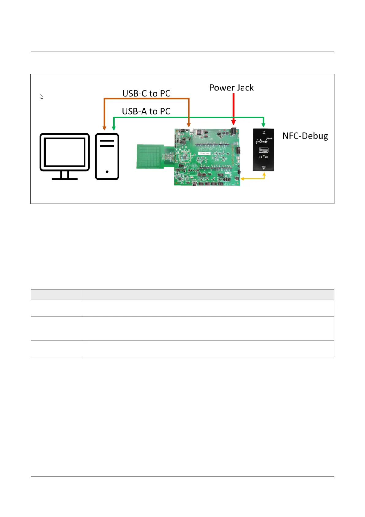
Figure 2. System overview - PN76 and external debugger
PNEV7642A connections:
• J5 "Top USB-C" connected with a USB-C cable to the developers PC for communication (for example, VCOM
for NFC Cockpit).
• J9 "Power Jack" connected to a proper power supply to supply the PNEV7642A board.
– If your USB-C power is good enough (active USB Hub), you might power it directly via USB "J5" and not
with the power jack.
• J21 "NFC-Debug" to connect a Debug Probe like a SEGGER J-Link, MCU-Link, or LPC-Link2. To flash and
debug the PN76.
What Why
PNEV7642A Board The PNEV7642A is the evaluation board of the PN7642 chipset. This whole document describes how
to configure and program it.
Debug Probe In the picture above, a SEGGER J-Link is shown as external debugger. If you want to flash an
application and debug it, onto the PN7642, you need an external debug probe. This can either be a
LPC-Link2, MCU-Link, or a SEGGER J-Link.
Personal Computer
(Host)
A Windows, Linux, or MacOS computer is necessary to run the IDE for developing applications for the
PN7640 chip. Currently only Windows is fully supported and described within this application note.
Table 2. Boards and utility overview
1.2.3 PN76, LPC55, and external debugger
Following shall indicate how an evaluation setup with PNEV7642A, LPC55S16-EVK, and an external
programmer can look like.
AN13134 All information provided in this document is subject to legal disclaimers. © 2023 NXP B.V. All rights reserved.
Application note Rev. 2.5 — 2 May 2023
5 / 57

 Loading...


