NXP Semiconductors
AN13134
PN76 family evaluation board quick start guide
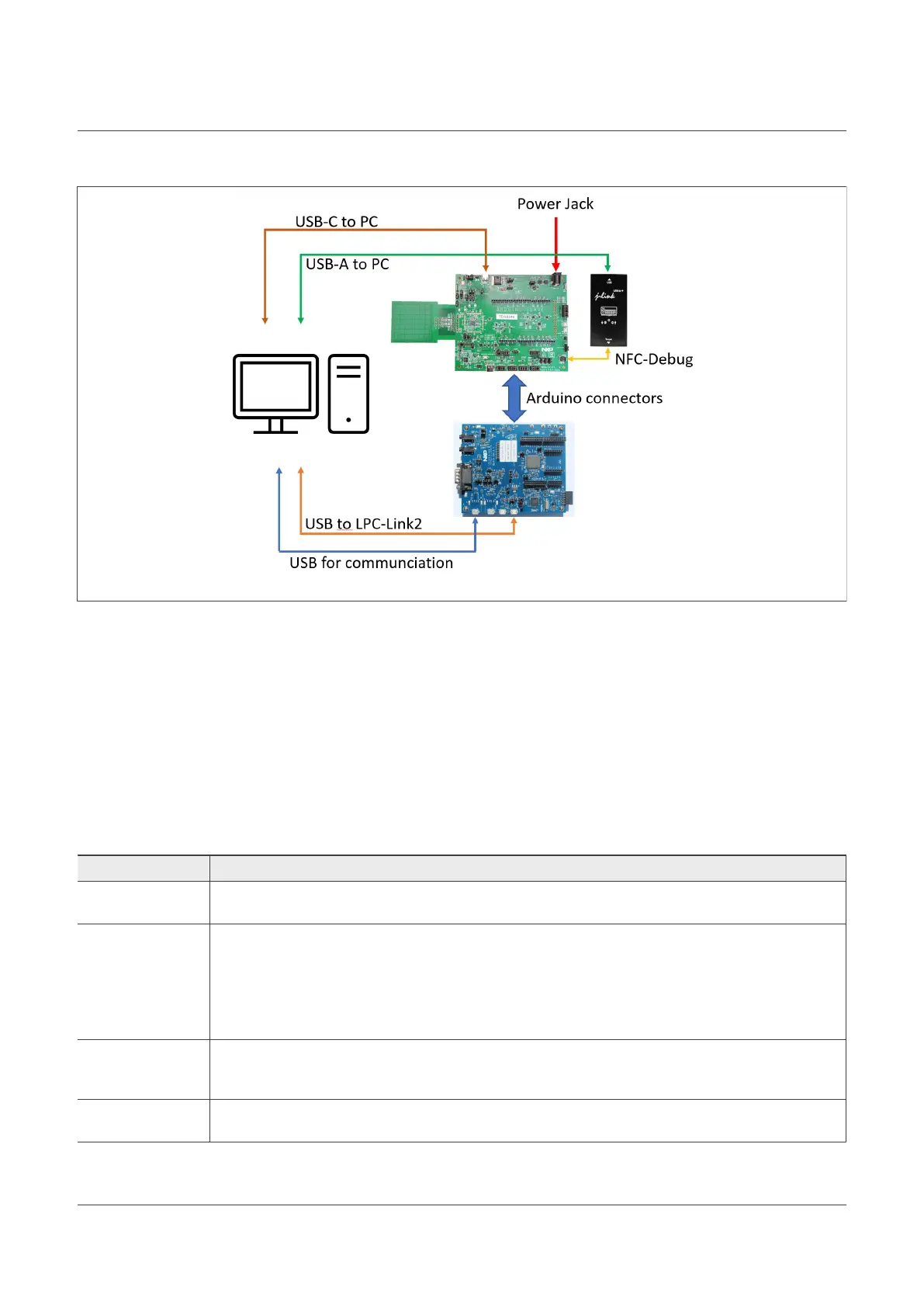
Figure 3. System overview
PNEV7642A connections:
• J5 "Top USB-C" connected with a USB-C cable to the developers PC for communication (for example, VCOM
for NFC Cockpit).
• J9 "Power Jack" connected to a proper power supply to supply the PNEV7642A board.
• J21 "NFC-Debug" to connect a Debug Probe, SEGGER J-Link or LPC-Link2, to program the PN76.
LPC55S16-EVK
• J4 "Main USB" connected to the PC for communication with the PC and/or as power supply for the
LPC55S16-EVK board.
• J1 "LINK2" connected to the PC and shown as LPC-Link2 debug probe. Used to program the LPC55S16.
What Why
PNEV7642A Board The PNEV7642A is the evaluation board of the PN7642 chipset. This whole document describes how
to configure and program it.
LPC55S16-EVK The LPC55S16-EVK is an optional board. It is only necessary for some of the provided examples like
HIF-based examples. The PNEV7642A is fully operational without this board.
Within the provided software package, you find "host software". This software is dedicated to run on
this LPC55S16 board to compliment another example running on the PNEV76FAMA board.
One of the major reasons to use a LPC55S16 besides showcasing the HIF encryption is to update
the PN7642 firmware. This currently cannot be done without the LPC55 board.
Debug Probe In the picture above, a SEGGER J-Link is shown as external debugger. If you want to flash an
application and debug it, onto the PN7642, you need an external debug probe. This can either be a
LPC-Link2 or a SEGGER J-Link.
Personal Computer
(Host)
A Windows, Linux, or MacOS computer is necessary to run the IDE for developing applications for the
PN7640 chip. Currently only Windows is fully supported and described within this application note.
Table 3. Boards and utility overview
AN13134 All information provided in this document is subject to legal disclaimers. © 2023 NXP B.V. All rights reserved.
Application note Rev. 2.5 — 2 May 2023
6 / 57

 Loading...


