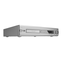
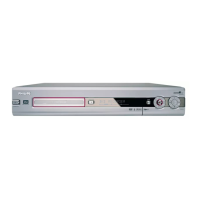
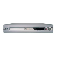
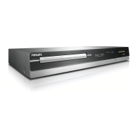
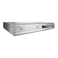
Circuit-, IC descriptions and list of abbreviations
EN 241DVDR70 & DVDR75/0x1 9.
9.13 List of Abbreviations
Analog Board
+5VSTBY .................... Permanent Supply 5V
8SC2 ............................ Pin8 Scart2 (only for Europe)
A_DATA ....................... Data from Analog- to Digital-Board
(UART-Communication)
A_RDY ......................... Analog-board ready (status
information to digital-board)
A18 - A19 ..................... Parallel Address Bus (CC - Flash-
ROM and S-RAM)
A8 - A17 ....................... Parallel Address Bus (CC - Flash-
ROM and S-RAM)
AD0 - AD7 .................... Parallel Address and Data Bus (CC -
Flash-ROM and S-RAM)
AFC .............................. Automatic Frequency Control
AFEL ............................ Audio Frontend Left
AFER............................ Audio Frontend Right
AGC / WSRI ................. Automatic Gain Control (for Europe),
Wide Screen Rear In (for NTSC)
AINFL ........................... Audio In Front Left
AINFR .......................... Audio In Front Right
AKILL ........................... Audio Kill Signal
ALADC ......................... Audio Left to ADC
ALDAC ......................... Audio Left from DAC
ALE .............................. Address Latch Enable
AM0.............................. Adress-mode 0
AM1.............................. Adress-mode 1
ARADC ........................ Audio Right to ADC
ARDAC ........................ Audio Right from DAC
ASCC1M...................... Audio Scart 1 Mute (System Clock
Output for Real time Clock-
Adjustment)
AVCC........................... Power Supply for A/D-converter
AVSS ........................... GND-Pin for A/D-converter
CFIN............................. Chroma Front In
CS0_............................ Chip Select 0 (CC - S-RAM)
CS2_............................ Chip Select 2 (CC - Flash-ROM)
CVBSFIN ..................... Video Front In
D_DATA....................... Data from Digital- to Analog-Board
(UART-Communication)
D_RDY......................... Digital-board ready (status information
from digital-board)
DAC_MUTE ................. Mute Signal for DAC
DAOUT ........................ Digital Audio Out
DVAL............................ Audio from Digital Video In Left
DVAR........................... Audio from Digital Video In Right
DVCC1......................... Power Supply Pin
DVCC2......................... Power Supply Pin
DVCC3......................... Power Supply Pin
DVSS1 ......................... GND Pin
DVSS2 ......................... GND Pin
DVSS3 ......................... GND Pin
FAN_OFF..................... Fan for Basic engine
ADV7196A
PIN FUNCTION DESCRIPTIONS
Pin Mnemonic Input/Output Function
1, 12 V
DD
P Digital Power Supply
2–11 Y0–Y9 I 10-Bit Progressive Scan/HDTV Input Port for Y Data. Input for G data when
RGB data is input.
13, 52 GND G Digital Ground
14–23 Cr0–Cr9 I
1
0-Bit Progressive Scan/HDTV Input Port for Color Data in 4:4:4 Input Mode.
In 4:2:2 mode this input port is not used. Input port for R data when RGB data
is input.
24, 35 V
AA
P Analog Power Supply
25 CLKIN I Pixel Clock Input. Requires a 27 MHz reference clock for standard operation in
Progressive Scan Mode or a 74.25 MHz (74.1758 MHz) reference clock in
HDTV mode.
26, 33 AGND G Analog Ground
27 DV I Video Blanking Control Signal Input
28 VSYNC/ I VSYNC, Vertical Sync Control Signal Input or TSYNC Input Control Signal in
TSYNC Async Timing Mode
29 HSYNC/ I HSYNC, Horizontal
Sync Control Signal Input or SYNC Input Control Signal in
SYNC
Async Timing Mode
30 SCL I MPU Port Serial Interface Clock Input
31 SDA I/O MPU Port Serial Data Input/Output
32 DAC C O Color Component Analog Output of Input Data on Cb/Cr9–0 Input Pins
34 DAC A O Y Analog Output
36 DAC B O Color Component Analog Output of Input Data on Cr9–Cr0 Input Pins
37 COMP O Compensation Pin for DACs. Connect 0.1 µF capacitor from COMP pin to V
AA
.
38 R
SET
I A 2470 Ω resistor (for input ranges 64–940 and 64–960; output standards
EIA-770.1–EIA-770.3) must be connected from this pin to ground and is used to
control the amplitudes of the DAC outputs. For input ranges 0–1023 (output
standards RS-170, RS-343A) the R
SET
value must be 2820 Ω.
39 V
REF
I/O Optional External Voltage Reference Input for DACs or Voltage Reference
Output (1.235 V)
40 RESET I This input resets the on-chip timing generator and sets the ADV7196A into
Default Register setting. Reset is an active low signal.
41 ALSB I TTL Address Input. This signal sets up the LSB of the MPU address. When this
pin is tied high, the I
2
C filter is activated which reduces noise on the I
2
C interface.
When this pin is tied low, the input bandwidth on the I
2
C interface is increased.
42–51 Cb/Cr9–0 I
1
0-Bit Progressive Scan/HDTV Input Port for Color Data. In 4:2:2 mode the
multiplexed CrCb data must be input on these pins. Input port for B data when
RGB is input.