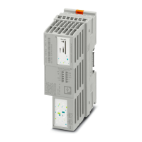
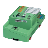
AXC F X152
36 / 112
PHOENIX CONTACT 107708_en_08
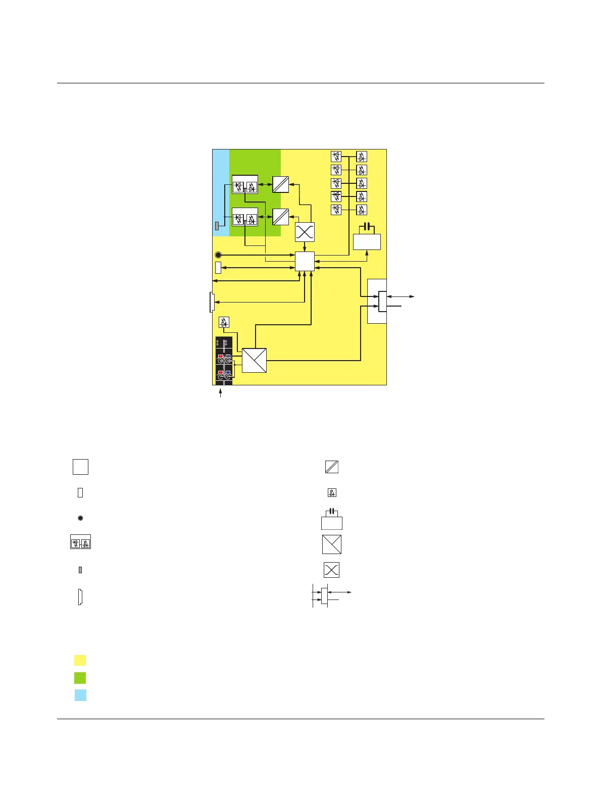
3.14 Internal basic circuit diagram
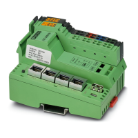
AXC F 1152 and AXC F 2152
Figure 3-15 Internal basic circuit diagram for AXC F 1152 and AXC F 2152
Key:
RJ45
RJ45
24 V
3.3 V
U
Bus
U
L
24 V
μC
RTC
LNK ACT
U
L
U
L
USB
Reset
FE
FAIL
RUN
BF-C
BF-D
SF
DBG
D
E
U
Bus
Local Bus
FE
Ethernet
LNK ACT
Extension
Bus
BOOT
EXT
SD
Microprocessor Transmitter
Service interface LED
Reset button Real-time clock
RJ45 interface Power supply unit
Functional ground connection Ethernet switch
SD card holder Axioline F local bus
Extension
bus
Left-aligned Axioline F extension modules
(AXC F 2152 only)
The colored areas in the basic circuit diagram represent electrically isolated areas:
Logic
Ethernet interface
Functional ground
 Loading...