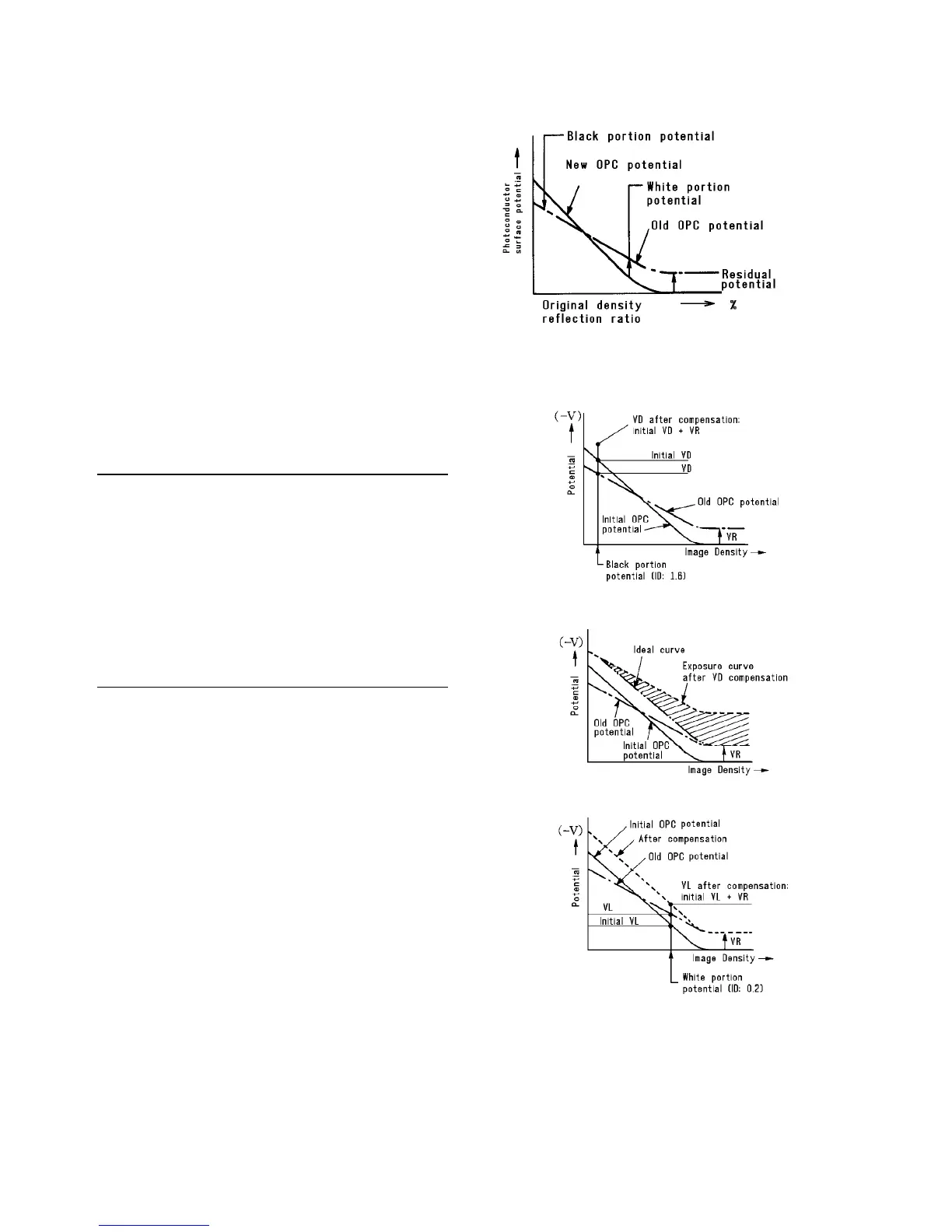
Old OPC potential curve
The photoconductor is given a specified surface
potential by charging. After that exposure forms a latent
image corresponding to the density of the original.
The surface potential after exposure varies with the
surface potential curve as shown in the figure on the
right. An old OPC’s potential curve is compared with
when the photoconductor is new. The black portion
potential drops and the white portion potential rises as a
result of photoconductor fatigue and change of the
operating environment (temperature and humidity). The
image contrast becomes lower and causes dirty
background of copy.
Compensation in latent image process
Latent image compensation keeps the difference in the
OPC potential between the black and white parts of the
pattern constant by changing the grid and flash outputs.
Black potential (VD) compensation
The residual potential (VR) is first measured by the OPC
potential sensor. Then the black latent image is formed
and the black potential (VD) is measured, if it is lower
than the "initial VD" + VR, the grid voltage is shifted up
until VD reaches the value of "initial VD" + VR. (The
"initial VD" is a target VD, which varies for each machine
and is set by service tool [4-01].) Therefore, VD after
compensation is increased by the residual potential (VR)
more than the initial VD.
White potential (VL) compensation
After VD compensation, the OPC has the same potential
curve as the old OPC potential curve; however the
curve has been shifted upward by the amount of VD
compensation.
The ideal curve has the same slope for forming the
correct latent image as the initial OPC potential curve,
so the potential shown by the diagonal lines is surplus.
VL compensation is done to delete this surplus.
During compensation, the white potential (VL) is
measured by the OPC potential sensor. Next, the flash
voltage is shifted up until VL reaches the initial VL + VR.
(The initial VL, called target VL, varies for each machine
and is set by service tool [4-01].)
VD and VL compensations are alternately done after
every 10 copies during a copying run. For VD
compensation, one step shift of the grid output is 28
volts, and 3 steps maximum shift at one time. For VL
compensation, 30 volts per 1 step and 3 steps maximum
shift at one time.
The grid and flash outputs are originally determined to
meet VD and VL with the target VD and VL. They are
called grid and flash setting steps. The amounts shifted
up or down for the compensation are called grid and
flash shift steps. All of them can be monitored with
service tool [4-01].
[V
D
]
[V
L
]
[V
R
]