U
sig
SHV inputs should exceed 10MΩ. A resistance value on the order of 1-2MΩ or less indicates a cabling error or a short on
the delay line. Please note that some other possible misconnections on the feedthrough may not be found by this test.
Likewise, the presence of shorts between other parts of the detector or from parts to ground will be revealed by a <10MΩ
“short” if measured through the SHV inputs of the decoupler circuits (assuming that all connections are in place). Exception:
between properly connected MCP front and MCP back input one can measure a resistance on the order of the expected MCP
stack resistance which may be <10MΩ in some cases, especially when the detector is still exposed to ambient air. In case of the
FT12TPhex please also refer to the next section for this test.
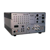
With the help of a fast signal pulse generator (e.g. the
RoentDek APG1) one can send a signal via an (output) lemo connector
(e.g. x1) of the FT12TP(hex) through a delay-line layer and verify the (delayed and slightly damped/distorted) response signal
from the (x2) output with an oscilloscope (see figure 2.6, the same check can be done for the other layers). Most wiring errors
will be revealed by a strongly distorted signal response.
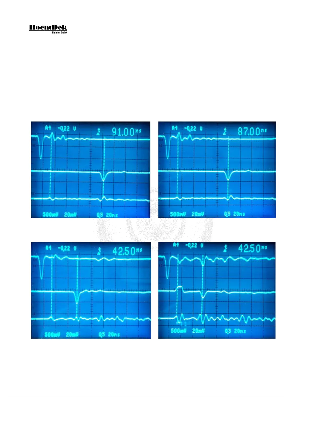
Figure 2.6: Response of a delay-line to a signal passing through a FT12TP(hex) plug. Upper trace: input signal,
middle trace: output signal from the opposing terminal of the same layer, lower trace: output from a terminal of
another layer (25x enlarged). The left marker defines the input time reference. Further explanations see text.
Figure 2.6 shows in the upper two images signals transmitted through the DLD80 anode layers via the FT12TP connector (left
picture: outer layer, i.e. via x
1
/x
2
, and inner layer on right picture). A correctly connected anode will show a slightly damped
output signal response (middle trace), delayed according to the delay-line transmission time (plus offset from connection cables).
The cross talk to another layer (lower trace) is small. The lower left image shows the same for a DLD40. If the connections
between pin 6 and 8 are swapped as in the right lower picture the response is clearly different.
Blocking resistors:
Page 28 of 83 MCP Delay Line Detector Manual (11.0.1304.1)