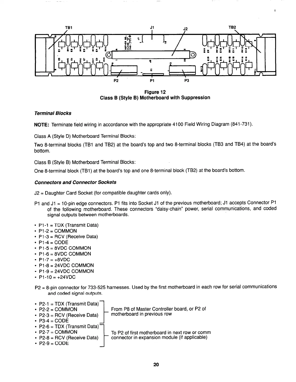
TBl
Jl
/
I
J2
TB2
\
P2
Pl
Figure 12
P3
Class B (Style B) Motherboard with Suppression
Terminal Blocks
NOTE:
Terminate field wiring in accordance with the appropriate 4100 Field Wiring Diagram (841-731).
Class A (Style D) Motherboard Terminal Blocks:
Two 8-terminal blocks (TBl and TB2) at the board’s top and two 8-terminal blocks (TB3 and TB4) at the board’s
bottom.
Class B (Style B) Motherboard Terminal Blocks:
One 8-terminal block (TBl) at the board’s top and one 8-terminal block (TB2) at the board’s bottom.
Connectors and Connector Sockets
J2 = Daughter Card Socket (for compatible daughter cards only).
Pl and Jl = lo-pin edge connectors. Pl fits into Socket Jl of the previous motherboard; Jl accepts Connector Pl
of the following motherboard. These connectors “daisy-chain” power, serial communications, and coded
signal outputs between motherboards.
l
Pl-1 = TDX (Transmit Data)
l
Pl-2 = COMMON
l
Pl -3 = RCV (Receive Data)
l
Pl-4 = CODE
l
Pl-5 = 8VDC COMMON
l
Pl-6 = 8VDC COMMON
l
Pi -7 = +8VDC
l
Pl-8 = 24VDC COMMON
l
Pl-9 = 24VDC COMMON
l
Pl-10 = +24VDC
P2 = 8-pin connector for 733-525 harnesses. Used by the first motherboard in each row for serial communications
and coded signal outputs.
l
P2-1 = TDX (Transmit Data)
l
P2-2 = COMMON
l
P2-3 = RCV (Receive Data)
l
P3-4 = CODE
1
From P8 of Master Controller board,.or P2 of
motherboard in previous row
l
P2-6 = TDX (Transmit Data)
l
P2-7 = COMMON
l
P2-8 = RCV (Receive Data)
l
P2-9 = CODE
l-
To P2 of first motherboard in next row or comm
connector in expansion module (if applicable)
20