4747
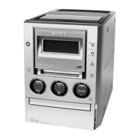
HCD-M333
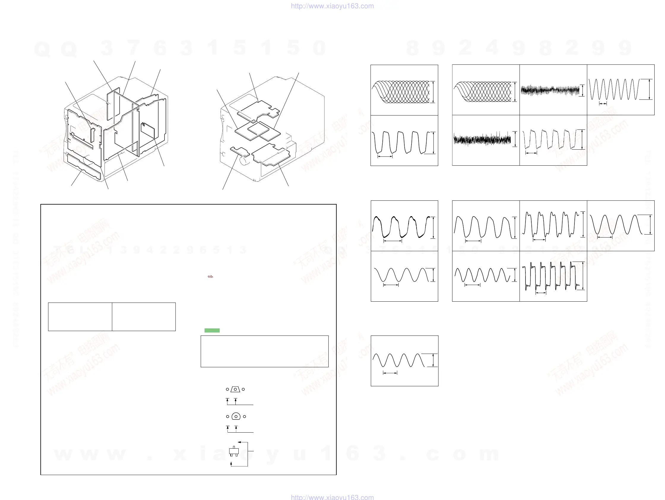
• Waveforms
1 IC103 qg (RFAC)
(PLAY mode)
2 IC101 us (XTAO)
1.2 Vp-p
200mV/DIV, 400ns/DIV
29.5 ns
4.4 Vp-p
1V/DIV, 10ns/DIV
3
IC101 ek (RF)
(PLAY mode)
1.4 Vp-p
500 mV/DIV, 200 ns
4
IC101 ef (FE)
(PLAY mode)
approx.
460 mVp-p
200 mV/DIV, 20 ms/DIV
5
IC101 wh (TE)
(PLAY mode)
200 mV/DIV, 20 ms/DIV
approx.
620 mVp-p
88.6 ns
4.3 Vp-p
6
IC803 8 (XOUT)
1 V/DIV, 40 ns/DIV
5.5 ns
3.3 Vp-p
7
IC801 5 (CLKA)
1V/DIV, 4 ns/DIV
8 IC101 qa (XCOUT)
9 IC101 qd (XOUT)
3.6 Vp-p
1 V/DIV, 10
µ
s/DIV
62.6 ns
2.8 Vp-p
1 V/DIV, 20 ns/DIV
30.5
µ
s
q; IC702 9 (XCOUT)
qa IC702 qa (XOUT)
3.7 Vp-p
1V/DIV, 10
µ
s/DIV
100 ns
3.7 Vp-p
1 V/DIV, 40 ns/DIV
30.5
µ
s
qs IC752 5
qd IC703 wd (XI)
4.5 Vp-p
1V/DIV, 40ns/DIV
167 ns
4.8 Vp-p
1V/DIV, 100ns/DIV
83ns
qf IC704 ws (XO)
3.5 Vp-p
1V/DIV, 40ns/DIV
100ns
12
µ
s
12.5 Vp-p
5 V/DIV, 4
µ
s/DIV
qg Q642 collector (TAPE REC)
6-1. Circuit Boards Location
MAIN BOARD
PANEL BOARD
T/C BOARD
BD(MD) BOARD
LOADING BOARD
BD(CD) BOARD
MD DIGITAL BOAR
H/P BOARD
LED BOARD
REG BOARD
POWER BOARD
AMP BOARD
TRANS BOARD
SECTION 6
DIAGRAMS
THIS NOTE IS COMMON FOR PRINTED WIRING
BOARDS AND SCHEMATIC DIAGRAMS.
(In addition to this, the necessary note is printed
in each block.)
For schematic diagrams.
Note:
• All capacitors are in µF unless otherwise noted. pF: µµF
50 WV or less are not indicated except for electrolytics
and tantalums.
• All resistors are in Ω and
1
/
4
W or less unless otherwise
specified.
•
f
: internal component.
• 5 : fusible resistor.
• C : panel designation.
For printed wiring boards.
Note:
• X : parts extracted from the component side.
• Y : parts extracted from the conductor side.
•
a
: Through hole.
• : Pattern from the side which enables seeing.
• A : B+ Line.
• B : B– Line.
• H : adjustment for repair.
•Voltages and waveforms are dc with respect to ground
under no-signal (detuned) conditions.
•Voltages are taken with a VOM (Input impedance 10 MΩ).
Voltage variations may be noted due to normal produc-
tion tolerances.
BD (CD) board
no mark : CD stop
BD (MD) board
no mark : MD stop
( ): MD playback
TC board
no mark : FM
( ): TAPE record
Other boards
no mark : FM
< > : CD stop
•Waveforms are taken with a oscilloscope.
Voltage variations may be noted due to normal produc-
tion tolerances.
• Indication of transistor
Caution:
Pattern face side: Parts on the pattern face side seen from
(SIDE B) the pattern face are indicated.
Parts face side: Parts on the parts face side seen from
(SIDE A) the parts face are indicated.
• Circled numbers refer to waveforms.
•Abbreviation
AUS: Australian model
CH : Chinese model
CND : Canadian model
HK
: Hong Kong model
• Signal path.
F : FM
J : CD
I : CD DIGITAL IN
E : PB (TAPE)
a : REC (TAPE)
p : PB (MD)
l : REC (MD)
J : USB
B
These are omitted.
CE
B
These are omitted.
CE
C
B
These are omitted.
E
Q
BD (CD) Board BD (MD) Board
MD DIGITAL BoardMAIN Board
TC Board
Ver 1.1 2003.05
The components identified by
mark 0 or dotted line with mark
0 are critical for safety.
Replace only with part number
specified.
Les composants identifiés par
une marque 0 sont critiques
pour la sécurité.
Ne les remplacer que par une
pièce portant le numéro spécifié.
w
w
w
.
x
i
a
o
y
u
1
6
3
.
c
o
m
Q
Q
3
7
6
3
1
5
1
5
0
9
9
2
8
9
4
2
9
8
T
E
L
1
3
9
4
2
2
9
6
5
1
3
9
9
2
8
9
4
2
9
8
0
5
1
5
1
3
6
7
3
Q
Q
TEL 13942296513 QQ 376315150 892498299
TEL 13942296513 QQ 376315150 892498299
http://www.xiaoyu163.com
http://www.xiaoyu163.com