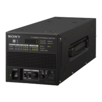
80
NETWORK TRUNK signal
The NETWORK TRUNK signal from the RJ-45 connector on the CN-4132 board is input from the connector (CN601) to IC601 in
which the signal format is converted. Then the converted signal is input to IC1101. Packet data that passes this connector can be
included in the Link-B data of the serial digital video signal, enabling transmission and reception of the NETWORK TRUNK packet
to/from the camera.
REFERENCE signal
The Reference connector can input the SD Black Burst signal and the HD ternary sync signal. The reference signal is input from the
BNC connector (J801).
The Sync Separator (IC811) on the VIF-82 board removes color burst and serration pulses to extract V-Sync (HD/SD-TEMP-V) and
H-Sync (HD/SD-TEMP-H) signals.
IC1101 monitors HD/SD-TEMP-V and HD/SD-TEMP-H signals and verifies the effectiveness as a video synchronization signal.
When a correct reference signal is input, IC1101, phase comparator (IC906), and VCO (VC904) generate a 27 MHz clock signal
locked to the input reference signal.
If the reference signal is not input, VC904 oscillates itself to generate a 27 MHz clock signal.
The VC904 input voltage is converted to a digital signal in IC1003 so that it can be read by the CPU. This value is proportional to the
27 MHz reference clock frequency.
IC1101, IC905, and VC902/VC903 generate a 148.5/148.35 MHz clock signal locked to a frequency of 27 MHz. These components
divide the 148.5/148.35 MHz clock to generate a 74.25/74.176 MHz clock signal locked to a frequency of 27 MHz.
IC1101, IC907, and VC901 generate a 24.576 MHz (512 fs) clock locked to a frequency of 27 MHz.
Thus a reference clock for HD video and audio signals is generated.
Furthermore, IC1101 generates reference synchronization signals (MST-HD-F, MST-HD-H, MST-SD-F, and MST-SD-H) using the
27 MHz, 74.25/74.176 MHz, HD/SD-TEMP-V, and HD/SD-TEMP-H signals.
By using the reference synchronization signals (MST-HD-F, MST-HD-H, MST-SD-F, and MST-SD-H), the 27 MHz clock,
148.5/148.35 MHz clock, and 74.25/74.176 MHz clock are distributed from IC913, IC915, and IC914 respectively. Then these clock
signals are delivered to the circuits in the unit.
Power unit interface
IC1101 monitors and controls the power unit through the I2C interface. IC1101 is connected through the connector (CN001).
Front panel interface
The VIF-82 board located between the CPU (AT-195 board) and the front panel (FP-322 board) functions as an IO expander to
control switches and LEDs.
The value (F_INC_VR) of the potentiometer on the front panel is converted to digital data in IC1003 so that it can be read by the
CPU.