DocID13902 Rev 15 164/1128
RM0008 General-purpose and alternate-function I/Os (GPIOs and AFIOs)
195
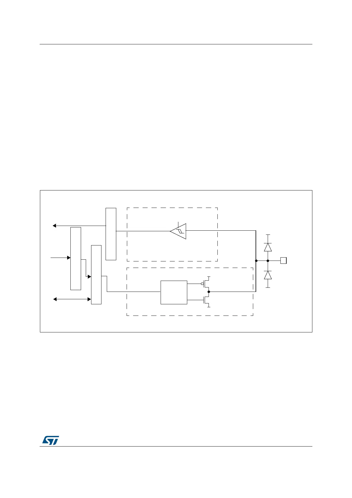
9.1.8 Output configuration
When the I/O Port is programmed as Output:
• The Output Buffer is enabled:
– Open Drain Mode: A “0” in the Output register activates the N-MOS while a “1” in
the Output register leaves the port in Hi-Z. (the P-MOS is never activated)
– Push-Pull Mode: A “0” in the Output register activates the N-MOS while a “1” in the
Output register activates the P-MOS.
• The Schmitt Trigger Input is activated.
• The weak pull-up and pull-down resistors are disabled.
• The data present on the I/O pin is sampled into the Input Data Register every APB2
clock cycle
• A read access to the Input Data Register gets the I/O state in open drain mode
• A read access to the Output Data register gets the last written value in Push-Pull mode
The Figure 16 on page 164 shows the Output configuration of the I/O Port bit.
Figure 16. Output configuration
1. V
DD_FT
is a potential specific to five-volt tolerant I/Os and different from V
DD
.
Push-pull or
Open-drain
Output
control
I/O pin
V
DD
V
SS
TTL Schmitt
trigger
V
SS
V
DD
or V
DD_FT
(1)
Protection
diode
Protection
diode
on
Input driver
Output driver
P-MOS
N-MOS
Input data register
Output data register
Read/write
Read
Bit set/reset registers
Write
ai14784
 Loading...


