Flexible static memory controller (FSMC) RM0008
503/1128 DocID13902 Rev 15
HADDR[25:0] contain the external memory address. Since HADDR is a byte address
whereas the memory is addressed in words, the address actually issued to the memory
varies according to the memory data width, as shown in the following table.
Wrap support for NOR Flash/PSRAM
Wrap burst mode for synchronous memories is not supported. The memories must be
configured in linear burst mode of undefined length.
21.4.2 NAND/PC Card address mapping
In this case, three banks are available, each of them divided into memory spaces as
indicated in Table 102.
For NAND Flash memory, the common and attribute memory spaces are subdivided into
three sections (see in Table 103 below) located in the lower 256 Kbytes:
• Data section (first 64 Kbytes in the common/attribute memory space)
• Command section (second 64 Kbytes in the common / attribute memory space)
• Address section (next 128 Kbytes in the common / attribute memory space)
10 Bank 1 - NOR/PSRAM 3
11 Bank 1 - NOR/PSRAM 4
1. HADDR are internal AHB address lines that are translated to external memory.
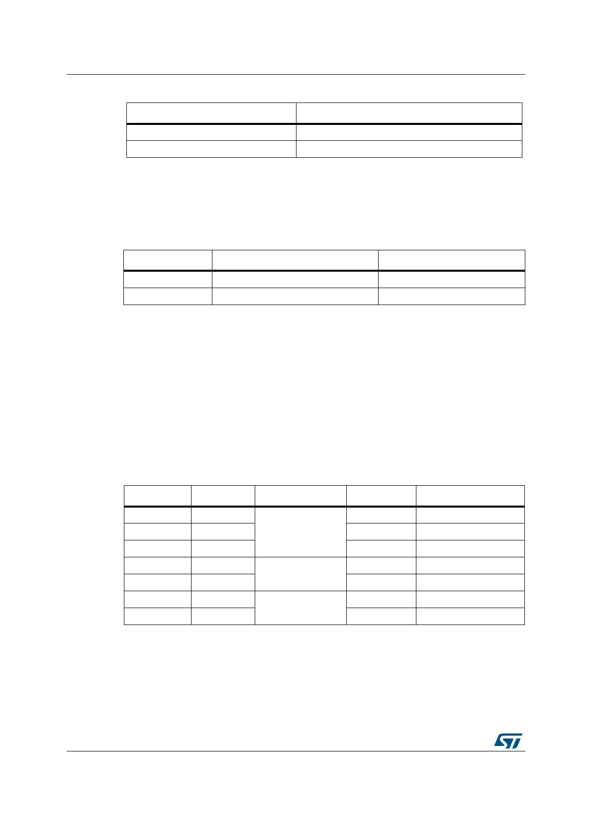
Table 101. External memory address
Memory width
(1)
1. In case of a 16-bit external memory width, the FSMC will internally use HADDR[25:1] to generate the
address for external memory FSMC_A[24:0].
Whatever the external memory width (16-bit or 8-bit), FSMC_A[0] should be connected to external memory
address A[0].
Data address issued to the memory Maximum memory capacity (bits)
8-bit HADDR[25:0] 64 Mbytes x 8 = 512 Mbit
16-bit HADDR[25:1] >> 1 64 Mbytes/2 x 16 = 512 Mbit
Table 100. NOR/PSRAM bank selection (continued)
HADDR[27:26]
(1)
Selected bank
Table 102. Memory mapping and timing registers
Start address End address FSMC Bank Memory space Timing register
0x9C00 0000 0x9FFF FFFF
Bank 4 - PC card
I/O FSMC_PIO4 (0xB0)
0x9800 0000 0x9BFF FFFF Attribute FSMC_PATT4 (0xAC)
0x9000 0000 0x93FF FFFF Common FSMC_PMEM4 (0xA8)
0x8800 0000 0x8BFF FFFF
Bank 3 - NAND Flash
Attribute FSMC_PATT3 (0x8C)
0x8000 0000 0x83FF FFFF Common FSMC_PMEM3 (0x88)
0x7800 0000 0x7BFF FFFF
Bank 2- NAND Flash
Attribute FSMC_PATT2 (0x6C)
0x7000 0000 0x73FF FFFF Common FSMC_PMEM2 (0x68)
 Loading...


