General-purpose timers (TIM9 to TIM14) RM0008
459/1128 DocID13902 Rev 15
16.5.9 TIM10/11/13/14 capture/compare register 1 (TIMx_CCR1)
Address offset: 0x34
Reset value: 0x0000
16.5.10 TIM10/11/13/14 register map
TIMx registers are mapped as 16-bit addressable registers as described in the tables below:
1514131211109876543210
CCR1[15:0]
rw rw rw rw rw rw rw rw rw rw rw rw rw rw rw rw
Bits 15:0 CCR1[15:0]: Capture/Compare 1 value
If channel CC1 is configured as output:
CCR1 is the value to be loaded in the actual capture/compare 1 register (preload value).
It is loaded permanently if the preload feature is not selected in the TIMx_CCMR1 register (bit
OC1PE). Else the preload value is copied in the active capture/compare 1 register when an
update event occurs.
The active capture/compare register contains the value to be compared to the counter
TIMx_CNT and signaled on OC1 output.
If channel CC1is configured as input:
CCR1 is the counter value transferred by the last input capture 1 event (IC1).
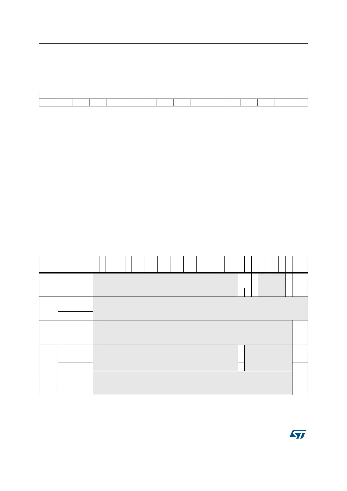
Table 93. TIM10/11/13/14 register map and reset values
Offset Register
31
30
29
28
27
26
25
24
23
22
21
20
19
18
17
16
15
14
13
12
11
10
9
8
7
6
5
4
3
2
1
0
0x00
TIMx_CR1
Reserved
CKD
[1:0]
ARPE
Reserved
URS
UDIS
CEN
Reset value 000 00 0
0x08
TIMx_SMCR
Reserved
Reset value
0x0C
TIMx_DIER
Reserved
CC1IE
UIE
Reset value 00
0x10
TIMx_SR
Reserved
CC1OF
Reserved
CC1IF
UIF
Reset value 000
0x14
TIMx_EGR
Reserved
CC1G
UG
Reset value 00
 Loading...


