DocID13902 Rev 15 964/1128
RM0008 Ethernet (ETH): media access control (MAC) with DMA controller
1064
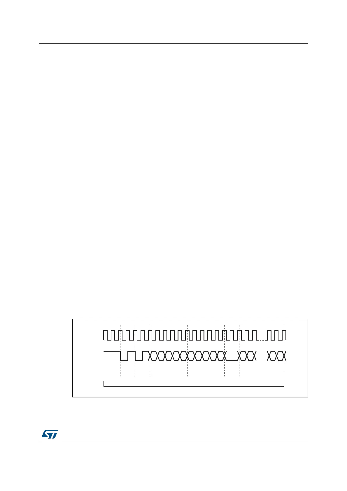
The management frame consists of eight fields:
• Preamble: each transaction (read or write) can be initiated with the preamble field that
corresponds to 32 contiguous logic one bits on the MDIO line with 32 corresponding
cycles on MDC. This field is used to establish synchronization with the PHY device.
• Start: the start of frame is defined by a <01> pattern to verify transitions on the line
from the default logic one state to zero and back to one.
• Operation: defines the type of transaction (read or write) in progress.
• PADDR: the PHY address is 5 bits, allowing 32 unique PHY addresses. The MSB bit of
the address is the first transmitted and received.
• RADDR: the register address is 5 bits, allowing 32 individual registers to be addressed
within the selected PHY device. The MSB bit of the address is the first transmitted and
received.
• TA: the turn-around field defines a 2-bit pattern between the RADDR and DATA fields
to avoid contention during a read transaction. For a read transaction the MAC controller
drives high-impedance on the MDIO line for the 2 bits of TA. The PHY device must
drive a high-impedance state on the first bit of TA, a zero bit on the second one.
For a write transaction, the MAC controller drives a <10> pattern during the TA field.
The PHY device must drive a high-impedance state for the 2 bits of TA.
• Data: the data field is 16-bit. The first bit transmitted and received must be bit 15 of the
ETH_MIID register.
• Idle: the MDIO line is driven in high-impedance state. All three-state drivers must be
disabled and the PHY’s pull-up resistor keeps the line at logic one.
SMI write operation
When the application sets the MII Write and Busy bits (in Ethernet MAC MII address register
(ETH_MACMIIAR)), the SMI initiates a write operation into the PHY registers by transferring
the PHY address, the register address in PHY, and the write data (in Ethernet MAC MII data
register (ETH_MACMIIDR). The application should not change the MII Address register
contents or the MII Data register while the transaction is ongoing. Write operations to the MII
Address register or the MII Data Register during this period are ignored (the Busy bit is
high), and the transaction is completed without any error. After the Write operation has
completed, the SMI indicates this by resetting the Busy bit.
Figure 328 shows the frame format for the write operation.
Figure 328. MDIO timing and frame structure - Write cycle
MDC
MDIO
32 1's 0 1
0
1
A4 A3 A2 A1 A0 R4 R3 R2 R1 R0
D15 D14
D1 D0
Preamble
Start
of
frame
OP
code
PHY address Register address
Turn
around
data
Data to PHY
ai15626
 Loading...


