Debug support (DBG) RM0008
1073/1128 DocID13902 Rev 15
Note: When the APB bridge write buffer is full, it takes one extra APB cycle when writing the
AFIO_MAPR register. This is because the deactivation of the JTAGSW pins is done in two
cycles to guarantee a clean level on the nTRST and TCK input signals of the core.
• Cycle 1: the JTAGSW input signals to the core are tied to 1 or 0 (to 1 for nTRST, TDI
and TMS, to 0 for TCK)
• Cycle 2: the GPIO controller takes the control signals of the SWJTAG IO pins (like
controls of direction, pull-up/down, Schmitt trigger activation, etc.).
31.4.3 Internal pull-up and pull-down on JTAG pins
It is necessary to ensure that the JTAG input pins are not floating since they are directly
connected to flip-flops to control the debug mode features. Special care must be taken with
the SWCLK/TCK pin which is directly connected to the clock of some of these flip-flops.
To avoid any uncontrolled IO levels, the device embeds internal pull-ups and pull-downs on
the JTAG input pins:
• NJTRST: Internal pull-up
• JTDI: Internal pull-up
• JTMS/SWDIO: Internal pull-up
• TCK/SWCLK: Internal pull-down
Once a JTAG IO is released by the user software, the GPIO controller takes control again.
The reset states of the GPIO control registers put the I/Os in the equivalent state:
• NJTRST: Input pull-up
• JTDI: Input pull-up
• JTMS/SWDIO: Input pull-up
• JTCK/SWCLK: Input pull-down
• JTDO: AF output floatingInput floating
The software can then use these I/Os as standard GPIOs.
Note: The JTAG IEEE standard recommends to add pull-ups on TDI, TMS and nTRST but there is
no special recommendation for TCK. However, for JTCK, the device needs an integrated
pull-down.
Having embedded pull-ups and pull-downs removes the need to add external resistors.
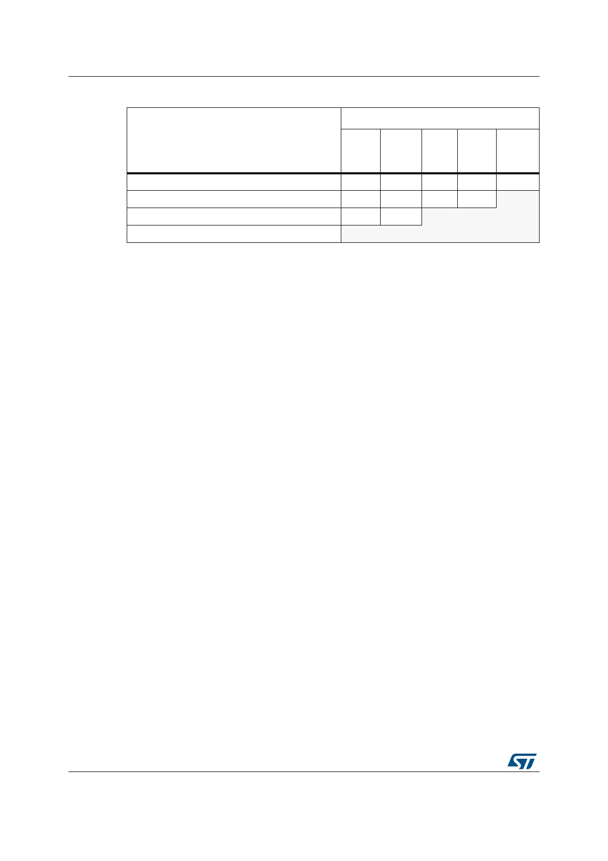
Table 219. Flexible SWJ-DP pin assignment
Available debug ports
SWJ IO pin assigned
PA13 /
JTMS /
SWDIO
PA14 /
JTCK /
SWCLK
PA15 /
JTDI
PB3 /
JTDO
PB4 /
NJTRST
Full SWJ (JTAG-DP + SW-DP) - Reset State X X X X X
Full SWJ (JTAG-DP + SW-DP) but without NJTRST X X X X
JTAG-DP Disabled and SW-DP Enabled X X
JTAG-DP Disabled and SW-DP Disabled Released
 Loading...


