Flexible static memory controller (FSMC) RM0008
505/1128 DocID13902 Rev 15
21.5.1 External memory interface signals
Table 105, Table 106 and Table 107 list the signals that are typically used to interface NOR
Flash, SRAM and PSRAM.
Note: Prefix “N”. specifies the associated signal as active low.
NOR Flash, nonmultiplexed I/Os
NOR Flash memories are addressed in 16-bit words. The maximum capacity is 512 Mbit (26
address lines).
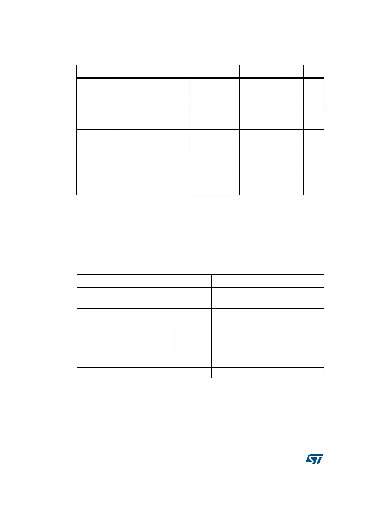
Table 104. Programmable NOR/PSRAM access parameters
Parameter Function Access mode Unit Min. Max.
Address
setup
Duration of the address
setup phase
Asynchronous
AHB clock cycle
(HCLK)
116
Address hold
Duration of the address hold
phase
Asynchronous,
muxed I/Os
AHB clock cycle
(HCLK)
216
Data setup
Duration of the data setup
phase
Asynchronous
AHB clock cycle
(HCLK)
2256
Bust turn
Duration of the bus
turnaround phase
Asynchronous and
synchronous read
AHB clock cycle
(HCLK)
116
Clock divide
ratio
Number of AHB clock cycles
(HCLK) to build one memory
clock cycle (CLK)
Synchronous
AHB clock cycle
(HCLK)
2 16
Data latency
Number of clock cycles to
issue to the memory before
the first data of the burst
Synchronous
Memory clock
cycle (CLK)
2 17
Table 105. Nonmultiplexed I/O NOR Flash
FSMC signal name I/O Function
CLK O Clock (for synchronous access)
A[25:0] O Address bus
D[15:0] I/O Bidirectional data bus
NE[x] O Chip select, x = 1..4
NOE O Output enable
NWE O Write enable
NL(=NADV) O
Latch enable (this signal is called address
valid, NADV, by some NOR Flash devices)
NWAIT I NOR Flash wait input signal to the FSMC
 Loading...


