Memory and bus architecture RM0008
51/1128 DocID13902 Rev 15
3.3 Memory map
See the datasheet corresponding to your device for a comprehensive diagram of the
memory map. Table 3 gives the boundary addresses of the peripherals available in all
STM32F10xxx devices.
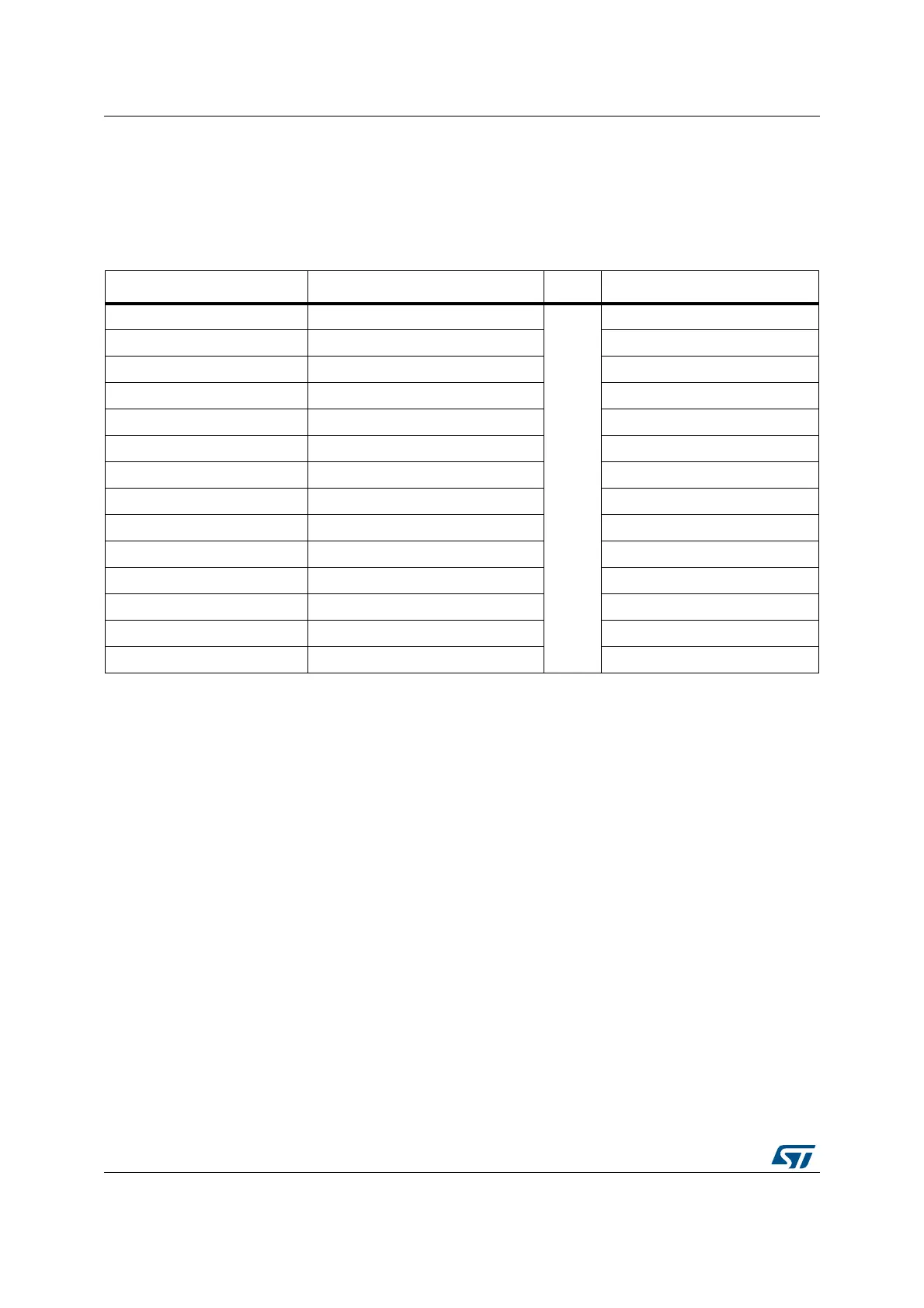
Table 3. Register boundary addresses
Boundary address Peripheral Bus Register map
0xA000 0000 - 0xA000 0FFF FSMC
AHB
Section 21.6.9 on page 554
0x5000 0000 - 0x5003 FFFF USB OTG FS Section 28.16.6 on page 905
0x4003 0000 - 0x4FFF FFFF Reserved
0x4002 8000 - 0x4002 9FFF Ethernet Section 29.8.5 on page 1061
0x4002 3400 - 0x4002 7FFF Reserved
0x4002 3000 - 0x4002 33FF CRC Section 4.4.4 on page 66
0x4002 2000 - 0x4002 23FF Flash memory interface
0x4002 1400 - 0x4002 1FFF Reserved
0x4002 1000 - 0x4002 13FF Reset and clock control RCC Section 7.3.11 on page 121
0x4002 0800 - 0x4002 0FFF Reserved
0x4002 0400 - 0x4002 07FF DMA2 Section 13.4.7 on page 289
0x4002 0000 - 0x4002 03FF DMA1 Section 13.4.7 on page 289
0x4001 8400 - 0x4001 FFFF Reserved
0x4001 8000 - 0x4001 83FF SDIO Section 1.9.16 on page 656
 Loading...


