Debug Clock
Debug Data
Dataissetuponthe
risingedgeofdebugclock.
Dataissampledbythe
receiveronthefalling
edgeofdebugclock.
T0302-01
Debug Clock
Debug Data
Start of Byte End of Byte
Time
T0303-01
Bit5
Bit7
Bit6
Bit4
Bit3
Bit2 Bit1
Bit0
Debug Mode
www.ti.com
3.1 Debug Mode
Debug mode is entered by forcing two falling-edge transitions on pin P2.2 (debug clock) while the
RESET_N input is held low. When RESET_N is set high, the device is in debug mode.
On entering debug mode, the CPU is in the halted state with the program counter reset to address
0x0000.
While in debug mode, pin P2.1 is the debug-data bidirectional pin, and P2.2 is the debug-clock input pin.
NOTE: Note that the debugger cannot be used with a divided system clock. When running the
debugger, the value of CLKCONCMD.CLKSPD should be set to 000 when CLKCONCMD.OSC = 0 or
to 001 when CLKCONCMD.OSC = 1.
3.2 Debug Communication
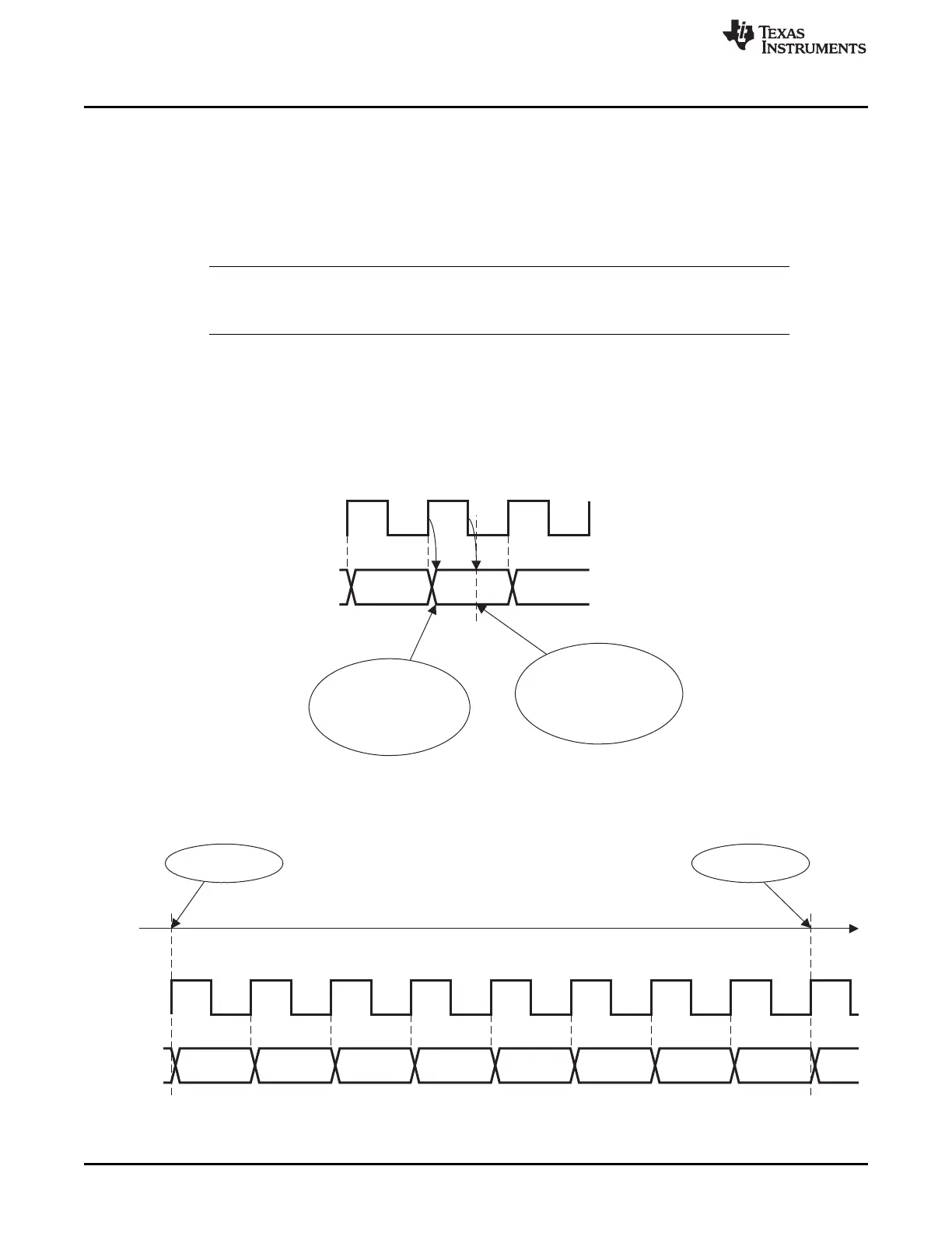
The debug interface uses a SPI-like two-wire interface consisting of the P2.1 (debug data) and P2.2
(debug clock) pins. Data is driven on the bidirectional debug-data pin at the positive edge of the debug
clock, and data is sampled on the negative edge of this clock.
The direction of the debug-data pin depends on the command being issued. Data is driven on the positive
edge of the debug clock and sampled on the negative edge. Figure 3-1 shows how data is sampled.
Figure 3-1. External Debug Interface Timing
The data is byte-oriented and is transmitted MSB-first. A sequence of one byte is shown in Figure 3-2.
Figure 3-2. Transmission of One Byte
54
Debug Interface SWRU191C–April 2009–Revised January 2012
Submit Documentation Feedback
Copyright © 2009–2012, Texas Instruments Incorporated
 Loading...


