2DA/2DB-1
2-3-21
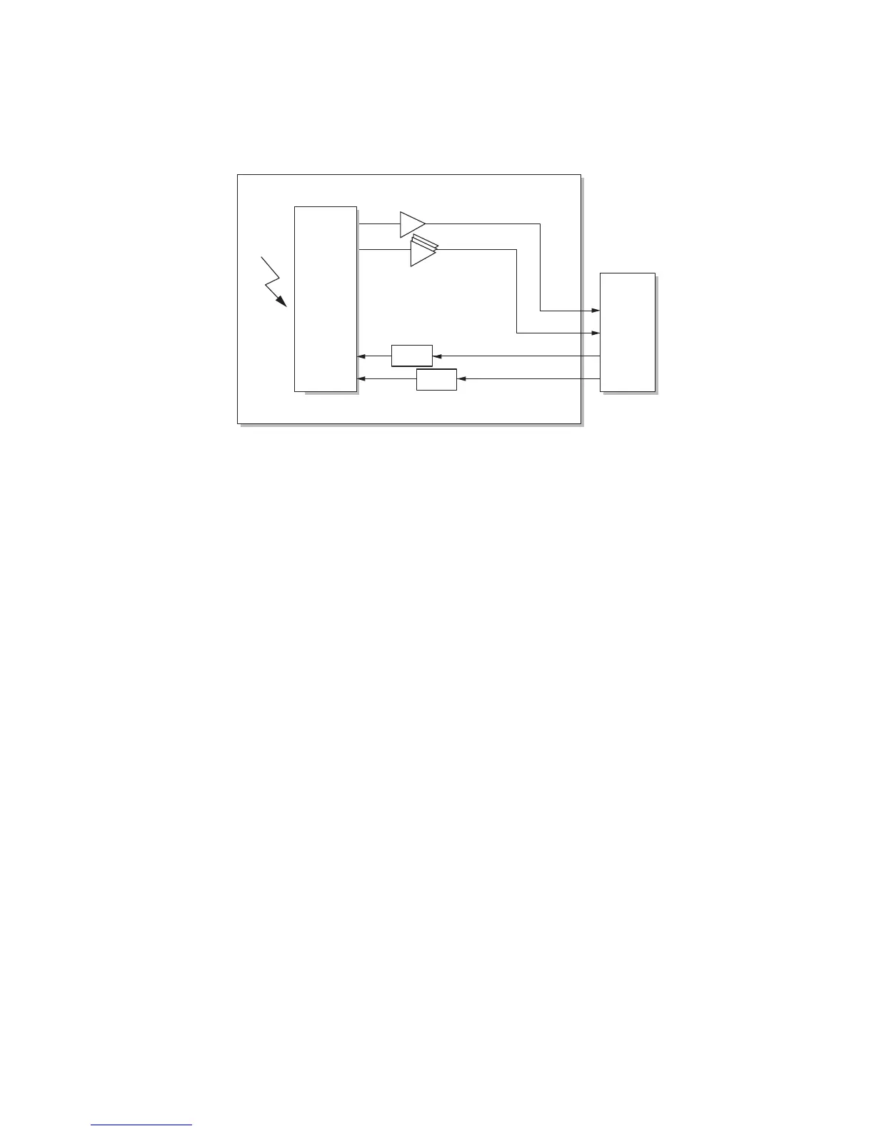
Figure 2-3-11 CCD PCB block diagram
The CCD PCB (CCDPCB) is equipped with a CCD sensor (U2) for original scanning.
The clock signals for driving the CCD sensor (U2) are sent from the main PCB (MPCB), and then input to the CCD sensor
(U2) via the clock drivers (U1 and U3).
Image signals are analog signals. Even- and odd-numbered pixels are output separately. These analog image signals are
amplified in the transistors (TR1 to 4) and then transmitted to the analog signal processing circuit in the main PCB (MPCB).
2-3-6 CCD PCB
MPCB
Tr.AMP
Driver
CCD sensor
U2
U1
U3
CCDPCB